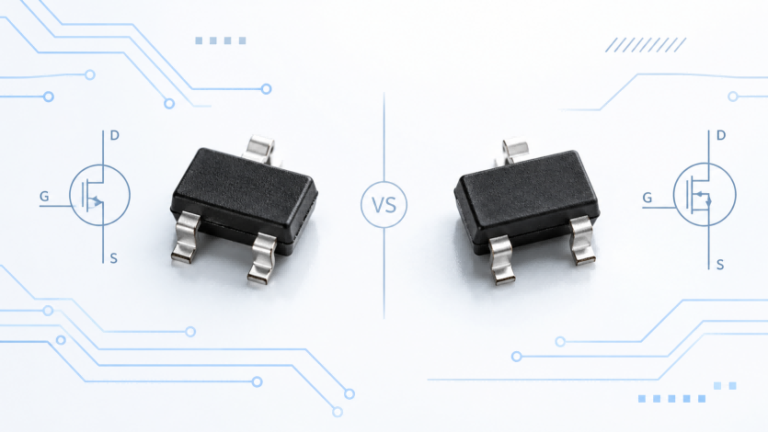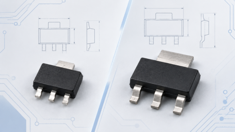
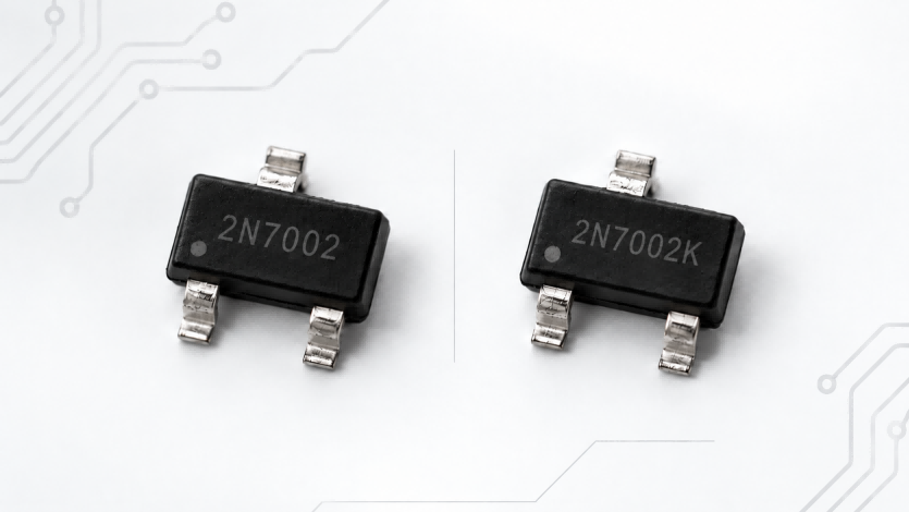
The 2N7002K and 2N7002 are N-channel enhancement-mode MOSFETs commonly available in SOT-23 packages for low-power switching applications. Their main differences often involve ESD protection, drain current capability, and drain-source on-resistance (RDS(on)). Many 2N7002K versions offer improved electrical performance, but the exact specifications depend on the manufacturer and part number.
A 2N7002K can often replace a standard 2N7002, provided the pinout, gate-drive voltage, electrical ratings, and thermal requirements are compatible. However, the reverse substitution requires particular care when the original design depends on enhanced ESD protection or lower on-resistance. This guide compares their key specifications and explains how to evaluate replacement compatibility in practical circuits.
What Are the Key Differences Between 2N7002K and 2N7002?
Both devices belong to the small-signal MOSFET category and operate as voltage-controlled switches. The 2N7002 is widely used in compact electronic circuits, while many 2N7002K variants provide improved on-state performance and additional gate protection. Their shared N-channel structure and common SOT-23 packaging make them suitable for similar applications, but they are not necessarily electrically identical.
The most useful comparison focuses on drain-source voltage, continuous drain current, on-resistance, gate threshold voltage, ESD protection, and power dissipation. These parameters determine how each MOSFET behaves under actual operating conditions and whether one device can safely replace another.
Electrical Specifications Comparison
The following table compares two representative SOT-23 devices using published electrical characteristics. The 2N7002K values follow datasheet 2N7002K/D, Rev. 20, while the standard 2N7002 values follow datasheet DS36649, Rev. 2-3. This is a comparison of specific implementations rather than a universal specification for every device carrying either base part number.
| Specification | 2N7002 | 2N7002K |
|---|---|---|
| MOSFET Type | N-Channel, Enhancement Mode | N-Channel, Enhancement Mode |
| Drain-Source Voltage (VDS) | 60 V | 60 V |
| Continuous Drain Current (ID) | 170 mA / 210 mA* | 320 mA / 380 mA* |
| RDS(on), Maximum | 7.5 Ω @ VGS = 5 V, ID = 50 mA | 2.5 Ω @ VGS = 4.5 V, ID = 200 mA |
| RDS(on) @ VGS = 10 V | 13.5 Ω maximum at TJ = 125°C, ID = 500 mA | 1.6 Ω maximum at TJ = 25°C, ID = 500 mA |
| Gate Threshold Voltage (VGS(th)) | 2.1–2.55 V @ ID = 250 µA, 25°C | 1.0–2.3 V @ ID = 250 µA, 25°C |
| Gate-Source Voltage (VGS), Continuous | ±20 V | ±20 V |
| ESD Protection | No enhanced ESD rating specified | Gate-source ESD protected, 2 kV HBM |
| Power Dissipation (PD) | 380 / 520 mW* | 300 / 420 mW* |
| Junction Temperature Range | -55°C to +150°C | -55°C to +150°C |
| Package | SOT-23 | SOT-23 |
The paired drain-current and power-dissipation values correspond to different PCB copper configurations at 25°C ambient. The figures are not direct same-board comparisons. RDS(on) values also use different test conditions and should not be interpreted as a universal performance ratio.
The comparison shows that the selected 2N7002K provides lower specified on-resistance and higher continuous drain-current ratings under its documented conditions. Both devices have a 60 V drain-source rating, but their gate characteristics, ESD robustness, and thermal performance differ. The standard 2N7002 also has different on-resistance limits at different temperatures, reinforcing the importance of comparing parameters under equivalent conditions.
The key takeaway is that 2N7002K is often an enhanced alternative to 2N7002, but the K suffix alone does not establish complete electrical compatibility. Even among devices with the same base part number, manufacturers may use different semiconductor processes, protection structures, and performance ratings.
ESD Protection and the K Suffix
One important distinction is the protection of the MOSFET gate against electrostatic discharge. The gate oxide in a MOSFET is sensitive to excessive voltage, and static electricity during handling or assembly can damage the device. Some 2N7002K versions incorporate an internal gate-to-source protection network that helps limit potentially damaging voltage transients.
For example, the 2N7002K implementation described in datasheet 2N7002K/D includes gate-source ESD protection rated at 2,000 V under the Human Body Model (HBM) test method. This provides a documented level of electrostatic-discharge robustness. However, an ESD rating is not the same as protection against sustained overvoltage, inductive load transients, or high-energy supply surges.
The K suffix should not be treated as a universal industry-defined performance grade. While it identifies enhanced characteristics in certain product families, the exact meaning depends on the manufacturer’s device designation. Likewise, a standard 2N7002 should not automatically be assumed to have no ESD protection. For component replacement, the actual ESD specification and protection requirements are more important than the suffix itself.
Current Capability, On-Resistance, and Power Loss
Drain-source on-resistance, or RDS(on), determines how much resistance the MOSFET presents when its channel is sufficiently enhanced. Lower RDS(on) generally reduces voltage drop and conduction losses at the same drain current, making it particularly useful in switching circuits where efficiency and temperature rise matter.
The approximate conduction loss can be calculated as:
Pcond ≈ ID² × RDS(on)
For example, assume a MOSFET carries 200 mA continuously while fully enhanced. If its effective RDS(on) is 2.5 Ω, the calculated conduction loss is approximately 0.10 W. At 7.5 Ω, the same current would produce approximately 0.30 W. These are illustrative calculations at assumed resistance values, not guaranteed operating results for the devices in the table, because their published resistance limits apply at different gate voltages and test currents.
Continuous drain-current ratings also require careful interpretation. A MOSFET rated for 380 mA does not necessarily support that current under every PCB layout or ambient temperature. The allowable operating current depends on junction temperature, PCB copper area, thermal resistance, and the power dissipated in the device. A small SOT-23 MOSFET may reach its thermal limit well before its nominal current rating becomes useful.
For this reason, higher current ratings and lower RDS(on) are meaningful advantages only when the actual gate-drive voltage and thermal conditions support them. Engineers should evaluate the expected operating point rather than selecting a MOSFET solely by the largest current value in its datasheet.
Can 2N7002K Replace 2N7002?
Yes, a 2N7002K can often replace a 2N7002, but it is not automatically a drop-in replacement. Both devices commonly use the same three-terminal SOT-23 format, and many 2N7002K implementations provide comparable voltage ratings with improved on-state performance. Nevertheless, reliable substitution requires confirmation of mechanical, electrical, and thermal compatibility.
For an existing PCB, the replacement must fit the original footprint, connect to the correct circuit nodes, and operate safely under the available gate-drive voltage and load current. Matching the package and nominal voltage rating is necessary, but these two conditions alone do not establish full compatibility.
Package and Pinout Compatibility
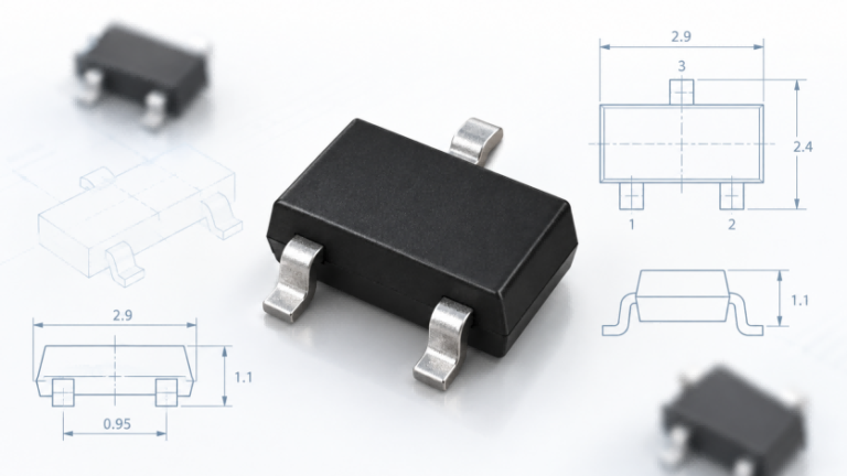
The common SOT-23 versions of 2N7002 and 2N7002K have three external terminals: Gate (G), Drain (D), and Source (S). In the two representative datasheets used above, the devices share the following terminal assignments when viewed according to their package drawings:
| Pin Number | Terminal | Function |
|---|---|---|
| 1 | Gate (G) | Controls MOSFET channel conduction |
| 2 | Source (S) | Source connection |
| 3 | Drain (D) | Drain connection |
This matching pin arrangement supports mechanical and electrical replacement between these particular implementations. However, SOT-23 describes a package format, not a universal electrical pin assignment. Engineers should verify the top-view orientation, terminal functions, package dimensions, and recommended PCB land pattern before substituting another manufacturer’s device.
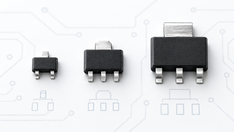
Understanding the broader SOT package family is useful when checking package drawings and footprints, especially when a proposed alternative uses a smaller or specialized variant. For direct PCB replacement, the actual component dimensions and terminal arrangement must agree with the existing design.
Electrical Compatibility and Replacement Direction
Replacing a standard 2N7002 with a 2N7002K is often feasible when both devices have compatible voltage ratings, pin assignments, and operating characteristics. A lower RDS(on) can reduce conduction losses, while enhanced ESD protection may improve handling robustness. However, the replacement must still operate correctly with the existing gate-drive voltage, switching frequency, and load conditions.
The reverse substitution requires particular attention. If a circuit was designed around a 2N7002K with low on-resistance or enhanced ESD protection, replacing it with a standard 2N7002 may increase conduction losses or remove a protection feature on which the design depends. The replacement may also have a lower current rating under the relevant thermal conditions.
The direction of substitution therefore matters, but it does not provide an automatic approval rule. In both cases, the following electrical characteristics should be verified:
- Drain-source voltage rating and required voltage margin.
- Maximum allowable gate-source voltage.
- RDS(on) at the available gate-drive voltage.
- Continuous and pulsed drain-current requirements.
- Power dissipation and junction-temperature limits.
- Gate leakage, ESD protection, and switching characteristics when relevant.
A device with apparently superior current and resistance specifications can still be unsuitable if its input characteristics or dynamic behavior differ significantly from those required by the circuit. This is particularly relevant in low-voltage logic systems and higher-frequency switching applications.
Practical Replacement Checklist
A reliable replacement assessment should begin with the existing circuit rather than the proposed part number. Identify the supply voltage, maximum load current, available gate-drive voltage, ambient temperature, and PCB thermal conditions. Then compare the candidate MOSFET against those requirements.
| Replacement Check | Required Verification |
|---|---|
| Package | Compatible SOT-23 outline and footprint |
| Pinout | Matching Gate, Drain, and Source assignments |
| VDS Rating | Sufficient for the maximum drain-source voltage, including expected transients |
| VGS Rating | Compatible with the gate-driver voltage range |
| Gate Drive | Adequate channel enhancement at the actual VGS |
| RDS(on) | Acceptable resistance and conduction loss under operating conditions |
| Drain Current | Adequate continuous and pulsed current capability |
| Thermal Performance | Junction temperature remains within limits |
| ESD Protection | Required protection level is maintained |
| Switching Behavior | Acceptable capacitance, gate charge, and switching performance |
Once these requirements have been established, an electronic parts cross-reference search can help identify possible alternatives for further datasheet comparison. Cross-reference results should be treated as candidates rather than automatically approved replacements.
For existing production equipment, especially when component substitution affects reliability or safety, final approval should include schematic verification and testing under representative operating conditions. A matching package and improved headline specifications do not eliminate the need to validate the replacement in the actual circuit.
3.3V Logic Drive and Practical Circuit Considerations
One of the most important considerations when using the 2N7002 or 2N7002K is whether the available gate-drive voltage is sufficient to turn the MOSFET fully on. Although both devices are commonly used in logic-controlled switching circuits, a low gate threshold voltage does not guarantee low on-resistance at 3.3 V. This distinction is particularly important when controlling loads directly from microcontroller GPIO pins.
The gate threshold voltage, VGS(th), indicates the voltage at which a small specified drain current begins to flow. It does not represent the voltage required for efficient switching at higher currents. For example, a MOSFET with a threshold voltage of 2 V may begin conducting at that voltage but still exhibit substantial drain-source resistance when driving a 100 mA or 200 mA load. Instead of relying on VGS(th), engineers should examine RDS(on) specifications and output characteristic curves at the available gate-drive voltage.
Consider a 3.3 V microcontroller controlling a 200 mA load through an N-channel MOSFET in a low-side switching configuration. If the device has an effective RDS(on) of 2.5 Ω at the operating gate voltage, its approximate conduction loss would be:
Pcond ≈ ID² × RDS(on) = 0.2² × 2.5 = 0.10 W
The corresponding drain-source voltage drop would be approximately 0.5 V. However, this calculation assumes that the MOSFET actually achieves 2.5 Ω at VGS = 3.3 V. A resistance specified at 4.5 V or 10 V cannot automatically be applied to a 3.3 V circuit. If the actual on-resistance is considerably higher, the voltage drop and power dissipation will increase. In extreme cases, insufficient gate drive can cause excessive heating or prevent the load from operating correctly.
A 5 V gate drive may provide stronger channel enhancement, but the appropriate voltage depends on the selected device and circuit architecture. For reliable 3.3 V operation, choose a MOSFET with suitable RDS(on) specifications at 2.5 V or 3 V when available, rather than assuming that every logic-level MOSFET will perform adequately. Higher-frequency switching circuits also require consideration of gate charge, input capacitance, and the microcontroller’s available drive capability.
Typical Applications and Selection Considerations
The 2N7002 and 2N7002K are commonly used for low-power switching, logic signal control, and voltage-level interfacing. Their compact surface-mount packages make them suitable for space-constrained PCB designs, while their N-channel enhancement-mode operation allows them to be controlled by appropriate digital logic signals. Typical applications include low-side switching, open-drain interfaces, signal switching, and low-current control circuits.
The most suitable device depends on the application requirements rather than the model suffix alone. In low-side load switching, gate-drive voltage, load current, and RDS(on) are important selection factors. In logic-level shifting and signal circuits, leakage current, voltage ratings, and switching characteristics may become more relevant. Applications involving frequent switching should also consider gate capacitance and switching losses.
For OEM projects requiring small-signal MOSFET sourcing or application-specific component selection, CNCHIPDEPOT supports semiconductor component sourcing and replacement evaluation. Selecting an appropriate MOSFET requires matching verified device characteristics to the electrical and environmental requirements of the application, rather than relying only on nominal part-number similarities.
Conclusion
The 2N7002K vs 2N7002 comparison shows that many 2N7002K versions offer lower on-resistance, higher drain-current capability, and enhanced ESD protection. However, these advantages vary by manufacturer and specific part number.
A 2N7002K can often replace a standard 2N7002 when the package, pinout, electrical ratings, and operating conditions are compatible. Before selecting either device, engineers should verify the actual gate-drive voltage, expected conduction losses, and thermal requirements. The safest replacement decision comes from comparing verified electrical characteristics rather than relying on the K suffix alone.
FAQs
The 2N7000 is commonly supplied in a TO-92 through-hole package, while the 2N7002 typically uses an SOT-23 surface-mount package. Both are N-channel enhancement-mode MOSFETs, but their pinouts, current ratings, and thermal characteristics may differ.
The gate threshold voltage depends on the specific 2N7002 manufacturer and version. It is commonly specified around 1–3 V at a very small drain current. VGS(th) indicates the beginning of conduction, not the voltage required for full enhancement.
Most standard 2N7002 MOSFETs have a maximum drain-source voltage rating of 60 V. This is an absolute maximum rating, not a recommended continuous operating voltage. The circuit should maintain an appropriate voltage margin.
Potential alternatives include compatible 2N7002K versions and selected BSS138 MOSFETs. However, equivalence depends on package, pinout, voltage ratings, RDS(on), gate-drive requirements, and thermal performance. These devices are not universally interchangeable.
The 2N7002 is an N-channel enhancement-mode MOSFET. Applying a sufficiently positive gate-source voltage creates a conductive channel between drain and source, allowing current to flow. Removing the gate drive turns the device off, apart from leakage current.