The SOT-23 package is a compact surface-mount semiconductor package commonly used for transistors, MOSFETs, diodes, and small ICs. A standard three-pin SOT-23 has typical body dimensions of approximately 2.9 × 1.3 × 1.0 mm, making it suitable for space-constrained PCB designs.
While SOT-23 commonly refers to the three-pin version, the package family also includes five-, six-, and eight-pin variants. Their lead arrangements, pin assignments, and PCB footprints are not necessarily interchangeable.
This guide explains SOT-23 dimensions, package types, pinout conventions, and footprint requirements, with practical guidance on identifying components and checking package compatibility.
What Is an SOT-23 Package?
SOT-23 stands for Small Outline Transistor, a miniature plastic semiconductor package designed for surface-mount technology (SMT). Unlike through-hole components, which have leads inserted through holes in a printed circuit board, SOT-23 devices are mounted directly onto surface pads. Their compact construction allows multiple components to fit into a relatively small PCB area while supporting automated electronic assembly.
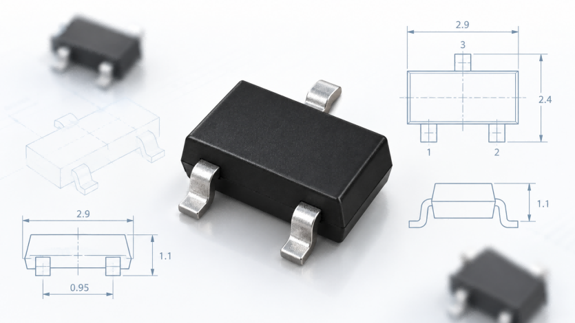
The standard SOT-23 package has three external terminals arranged along two sides of a rectangular body. It is commonly associated with the JEDEC TO-236AB package outline, with typical body dimensions of approximately 2.9 mm in length, 1.3 mm in width, and 1.0 mm in height. These dimensions describe the molded body rather than the complete mounting area required on a PCB.
| Feature | Standard SOT-23 |
|---|---|
| Package name | Small Outline Transistor |
| Package type | Surface-mount (SMD) |
| Typical body dimensions | 2.9 × 1.3 × 1.0 mm |
| Standard lead count | 3 |
| Lead arrangement | Two leads on one side, one on the opposite side |
| JEDEC package designation | TO-236AB |
| Common components | BJTs, MOSFETs, diodes, and protection devices |
| Mounting method | Surface-mount soldering |
Despite its name, SOT-23 is not exclusively a transistor package. The same physical format is used for switching diodes, Schottky diodes, MOSFETs, and other semiconductor devices. For example, the BAS16 switching diode uses a three-lead SOT-23 package for a single high-speed switching diode. This illustrates how a package originally associated with transistors can accommodate different electronic components.
The compact size and short external leads make SOT-23 suitable for dense PCB layouts and automated assembly. However, the package itself does not determine a component’s electrical characteristics, internal circuit, or pin functions. Those properties depend on the specific device and must be confirmed using its datasheet.
SOT-23 Package Dimensions and Drawings
The standard SOT-23 dimensions are approximately 2.9 mm in body length, 1.3 mm in body width, and 1.0 mm in height. These nominal measurements are useful for identifying the package and estimating its physical space requirements. However, actual package drawings specify dimensional ranges because manufactured components must accommodate mechanical tolerances.
An important distinction is the difference between the molded body dimensions and the overall dimensions including the leads. Since the terminals extend beyond the plastic housing, the component occupies more PCB space than its body measurements alone suggest. This difference matters when evaluating component clearance, mounting arrangements, and PCB footprint compatibility.
Standard SOT-23 Dimensions and Lead Spacing
The following table summarizes representative mechanical dimensions for the standard three-terminal SOT-23 package associated with the TO-236AB outline. All measurements are in millimeters.
| Parameter | Symbol | Minimum | Nominal | Maximum |
|---|---|---|---|---|
| Body length | D | 2.8 | 2.9 | 3.0 |
| Body width | E | 1.2 | 1.3 | 1.4 |
| Package height | A | 0.9 | 1.0 | 1.1 |
| Overall width including leads | HE | 2.1 | — | 2.5 |
| Same-side terminal spacing | e | — | 1.9 | — |
| Basic lead pitch reference | e1 | — | 0.95 | — |
| Lead width | bp | 0.38 | — | 0.48 |
Note: These are representative package-outline values, not universal manufacturing limits. Actual dimensional ranges and symbol definitions should be verified against the selected component’s mechanical drawing.
One detail that can cause confusion is the difference between 1.9 mm terminal spacing and 0.95 mm basic pitch. Both values may appear in SOT-23 technical documents, but they describe different geometric references.
In the standard three-pin configuration, the two terminals on the same side are separated by approximately 1.9 mm between their centerlines. The 0.95 mm value represents the underlying pitch reference used in certain package drawings. It should not be interpreted as the direct center-to-center distance between the two terminals on that side.
The overall package width also differs from the molded-body width because of the projecting terminals. For example, a body measuring approximately 1.3 mm wide may have an overall terminal-to-terminal width approaching 2.5 mm, depending on the specified outline and tolerances. These distinctions are important when working with compact circuit boards where small mechanical differences can affect component placement.
Understanding SOT-23 Package Drawings
An SOT-23 mechanical drawing generally includes top, side, and sometimes bottom views. Each view provides different information about the package geometry. Symbols such as D, E, and A identify dimensions such as body length, body width, and height, while additional symbols describe lead width, pitch, and terminal positioning.
The drawing should also establish the component’s terminal numbering and viewing orientation. This is especially important because a bottom-view diagram may appear reversed relative to the same component viewed from above. Confusing these orientations can lead to incorrect pin assignments when developing or checking a PCB layout.
Another important distinction is between a package outline drawing and a recommended PCB land pattern. The package outline describes the physical component, whereas the land pattern defines the copper pads used to mount it. The pad geometry must accommodate the component leads, dimensional tolerances, and intended soldering process rather than simply reproduce the body dimensions.
For engineering applications, nominal dimensions should be treated as reference information. The final mechanical specifications, terminal positions, and tolerances should be taken from the exact component’s datasheet or package drawing before completing a PCB design.
SOT-23 Package Types and Variants
Although the standard three-pin version is the most familiar, the broader SOT-23 package family includes configurations with different numbers of external leads. These variations accommodate semiconductor devices that require additional electrical connections while maintaining a relatively compact surface-mount format.
Names such as SOT-23-3, SOT-23-5, and SOT-23-6 generally indicate the number of leads associated with a particular package configuration. However, semiconductor packaging terminology is not completely uniform. Similar outlines may also appear under alternative package designations, so the name alone should not be treated as proof of mechanical compatibility.
SOT-23-3, SOT-23-5, SOT-23-6, and SOT-23-8
The following table summarizes four commonly documented variants within the SOT-23 family.
| Package | Lead Count | Typical Lead Spacing or Pitch | Common Component Types |
|---|---|---|---|
| SOT-23-3 | 3 | 1.9 mm between same-side leads | BJTs, MOSFETs, diodes |
| SOT-23-5 | 5 | 0.95 mm pitch | LDO regulators, op-amps, small ICs |
| SOT-23-6 | 6 | 0.95 mm pitch | Protection circuits, analog and control ICs |
| SOT-23-8 | 8 | 0.65 mm pitch | Selected multi-function ICs |
Note: The values represent commonly documented package configurations. Lead pitch, body dimensions, and package naming should be confirmed using the relevant device documentation.
SOT-23-3 is the standard three-terminal configuration and is frequently referred to simply as SOT-23. It has two leads on one side and a single lead on the opposite side. This format is widely used for discrete semiconductor components, including bipolar transistors, MOSFETs, and switching diodes.
SOT-23-5 increases the number of external connections to five, making it suitable for small integrated circuits requiring additional control or signal terminals. Typical examples include low-dropout voltage regulators and operational amplifiers. Depending on the device, the additional pins may support enable signals, feedback connections, or other functions.
SOT-23-6 provides six external terminals, commonly arranged as three leads on each side. This configuration is used for various compact analog, protection, and control devices. Although its overall form factor resembles other SOT-23 variants, the additional terminals require a different PCB pad arrangement.
SOT-23-8 accommodates eight external leads using a finer pitch, commonly around 0.65 mm in representative outlines. This allows more connections within a compact package but changes the terminal spacing and corresponding land-pattern requirements.
Package Names, Lead Arrangements, and Compatibility
SOT-23 package terminology can become confusing because similar mechanical outlines may have several designations. For example, SOT-23-5 may also appear as SOT-753 or SC-74A in certain technical documents, while SOT-23-6 may be associated with designations such as SOT-457 or SC-74.
These alternative names are useful when searching component datasheets and PCB library footprints. However, two packages with similar naming conventions are not necessarily interchangeable. Even when their molded-body dimensions overlap, the terminal arrangement, dimensional tolerances, or recommended solder pads may differ.
Another consideration is that the number of physical leads does not always equal the number of independent electrical connections. Some semiconductor devices internally connect multiple terminals to the same electrical node. Depending on the device, this arrangement may support current handling, thermal performance, or other design requirements.
For component selection, engineers should therefore verify the package outline, lead count, terminal arrangement, and recommended land pattern before deciding whether two devices can share a PCB footprint. The electrical functions of those terminals must then be checked separately against the individual component datasheets.
SOT-23 Pinout and Pin Configuration
The SOT-23 pinout depends on the semiconductor device contained inside the package. Although the standard SOT-23 configuration has three external terminals, the package designation does not define their electrical functions. A bipolar transistor, MOSFET, or diode array may use the same physical housing while assigning different electrical functions to its pins.
For example, a bipolar transistor requires emitter, base, and collector connections, while a MOSFET requires gate, source, and drain connections. A single-diode component may use only two terminals electrically, with another package lead unconnected. A dual-diode component may instead use all three terminals to access different points in its internal circuit. Therefore, a generic three-pin SOT-23 drawing cannot establish the correct electrical connections for every device.
A useful example is the BAV99 dual switching diode, which contains two series-connected diodes within a three-pin SOT-23 package. Unlike a single-diode device such as BAS16, BAV99 uses the external terminals to provide access to both ends and the intermediate connection of the diode pair. This illustrates how components with the same physical package can contain different internal electrical configurations.
For PCB design, testing, and component replacement, it is essential to distinguish pin numbering from electrical pin assignment. Pin numbering identifies the physical terminals, while the electrical pinout describes their actual functions. Always verify the component-specific pin diagram, including whether it uses a top or bottom view, before connecting the device to a circuit.
How Do You Choose the Correct SOT-23 Footprint?
A SOT-23 footprint defines the arrangement of copper pads used to mount a component onto a printed circuit board. While the package’s mechanical dimensions provide the basis for footprint selection, the pad geometry must also accommodate lead positioning, solder joint formation, and manufacturing tolerances. A suitable footprint helps ensure correct component alignment and reliable electrical connections during PCB assembly.
For a standard three-pin SOT-23 device, the footprint generally has two pads on one side and a single pad on the opposite side. However, five-pin and six-pin variants require different pad arrangements. Even when two components have similar body dimensions, differences in lead count, pitch, and terminal geometry may prevent them from sharing the same footprint.
The most reliable approach is to use the recommended PCB land pattern provided for the selected component. This drawing specifies the intended mounting pad geometry and terminal positions. Where no manufacturer-recommended pattern is available, designers may consult applicable industry land-pattern guidance, such as IPC-7351, and verify the resulting footprint against the component’s mechanical specifications.
| Design Factor | What to Check | Why It Matters |
|---|---|---|
| Package variant | SOT-23-3, SOT-23-5, SOT-23-6, etc. | Determines the required pad arrangement |
| Lead spacing | Center-to-center distance between terminals | Prevents alignment errors |
| Pad dimensions | Recommended pad length and width | Supports proper solder joint formation |
| Pin 1 orientation | Package drawing and PCB library orientation | Prevents incorrect placement |
| Solder mask clearance | Clearance around exposed copper pads | Reduces soldering defects |
| Thermal requirements | Power dissipation and PCB copper layout | Helps control operating temperature |
A common mistake in SOT-23 PCB layout is assuming that any library footprint labeled SOT-23 will fit every device using that designation. PCB libraries may contain similar footprint names with different pad dimensions or orientations. Before finalizing a design, engineers should compare the selected library footprint with the exact device package drawing rather than relying on its name alone.
Thermal performance is another important consideration. The small package provides limited physical area for transferring heat, so device power dissipation and PCB copper geometry can significantly affect junction temperature. The same package may have different allowable power dissipation values depending on the semiconductor device, board construction, ambient temperature, and operating conditions.
For production designs, the final footprint should therefore be checked against mechanical dimensions, pad recommendations, pin orientation, and relevant thermal requirements. This ensures that the selected component can be mounted correctly and operated within its specified limits.
SOT-23 Package and Component Identification
SOT-23 package identification begins with the component’s physical characteristics. A standard three-pin SOT-23 device has a small rectangular molded body with two terminals on one side and one on the opposite side. Comparing its body dimensions, terminal count, and lead arrangement with a package drawing can help distinguish it from other miniature surface-mount packages.
However, identifying the package does not necessarily identify the semiconductor device inside it. Two components can share the same SOT-23 outline while containing completely different internal circuits. One may be a transistor, another a MOSFET, and another a switching diode. The physical package only describes the external construction and cannot establish the component’s complete electrical identity.
Manufacturers commonly use short alphanumeric SOT-23 marking codes because the package surface is too small to display a complete part number. These markings may contain two or three characters, sometimes accompanied by production or identification codes. A marking is not necessarily unique across manufacturers, meaning that the same code may correspond to different semiconductor devices.
A practical identification process starts by examining the lead count and package dimensions, then recording the visible top marking. The next step is to search for possible component matches and compare their datasheets. The surrounding circuit can provide additional clues about the likely component function, but identification should ultimately be confirmed through the internal circuit, electrical specifications, and pin assignments.
For example, a small three-pin device located near a signal input could be a switching diode, transistor, or protection component, depending on the circuit. Its location alone is not sufficient evidence of its identity. Combining physical measurements, package markings, circuit context, and datasheet information provides a more reliable identification method.
How Does SOT-23 Compare with Similar Packages?
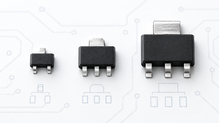
SOT-23 is frequently compared with other small-outline semiconductor packages, particularly SC70, SOT-323, and SOT-223. Some have similar external appearances, while others share the SOT naming convention despite significant differences in size and typical applications. Understanding these distinctions helps prevent incorrect package identification and PCB footprint selection.
SC70 and SOT-323 commonly refer to closely related miniature package outlines that are smaller than standard SOT-23. Their similar shapes can make identification difficult without checking actual dimensions, especially when components are already soldered onto densely populated PCBs. SOT-223, by contrast, is considerably larger and commonly used for devices requiring greater heat-dissipation capability.
| Feature | SOT-23 | SC70 / SOT-323 | SOT-223 |
|---|---|---|---|
| Typical body length | 2.9 mm | Approximately 2.0 mm | Approximately 6.5 mm |
| Typical body width | 1.3 mm | Approximately 1.25 mm | Approximately 3.5 mm |
| Common terminal arrangement | 3 leads | 3 leads | 3 leads plus a large tab |
| Relative size | Small | Smaller than SOT-23 | Larger than SOT-23 |
| Typical devices | Transistors, MOSFETs, diodes | Miniature transistors and diodes | Regulators and power transistors |
| PCB footprint | Standard SOT-23 pattern | Smaller land pattern | Larger land pattern with tab connection |
Note: Dimensions are representative of common package outlines. Exact measurements, pin arrangements, and footprint requirements must be confirmed for the specific device.
The main difference between SOT-23 and SC70/SOT-323 is their physical size and terminal spacing. Although they may contain similar types of semiconductor devices, their footprints are generally not interchangeable. Replacing one with the other may require a PCB layout change or a specifically designed adapter.
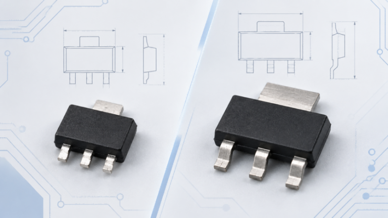
SOT-223 differs more substantially in physical construction. Its larger body and mounting tab can support higher power dissipation in suitable designs, making it common in some voltage regulators and power devices. However, actual thermal performance depends on the individual component, its thermal specifications, and the PCB copper area available for heat transfer.
Even when two components use exactly the same SOT-23 package, mechanical compatibility does not guarantee electrical interchangeability. Their pin assignments, polarity, voltage ratings, current limits, switching characteristics, or internal circuit configurations may differ. An electronic component cross-reference search can help identify potential alternatives, but each candidate must be checked against the original device’s datasheet and actual circuit requirements.
The SOT-23 package remains useful because of its compact footprint, compatibility with automated surface-mount assembly, and availability across many semiconductor categories. However, its small dimensions also introduce practical limitations involving thermal dissipation, component handling, and identification. Choosing the correct package therefore requires balancing physical dimensions with the electrical and manufacturing requirements of the application.
FAQs
SOT stands for Small Outline Transistor. SOT-23 identifies a compact surface-mount semiconductor package, commonly with three leads.
Usually, yes. SOT-23 commonly refers to the standard three-pin SOT-23-3 package. Verify the exact outline when selecting components.
No. SC70 is generally smaller than standard SOT-23 and requires different mechanical dimensions and PCB footprints.
Not necessarily. Compatible pinouts, electrical ratings, internal configurations, and operating requirements must all be verified.
Check the top marking, package dimensions, and pin count, then compare possible matches against component datasheets. Marking codes may not be unique.