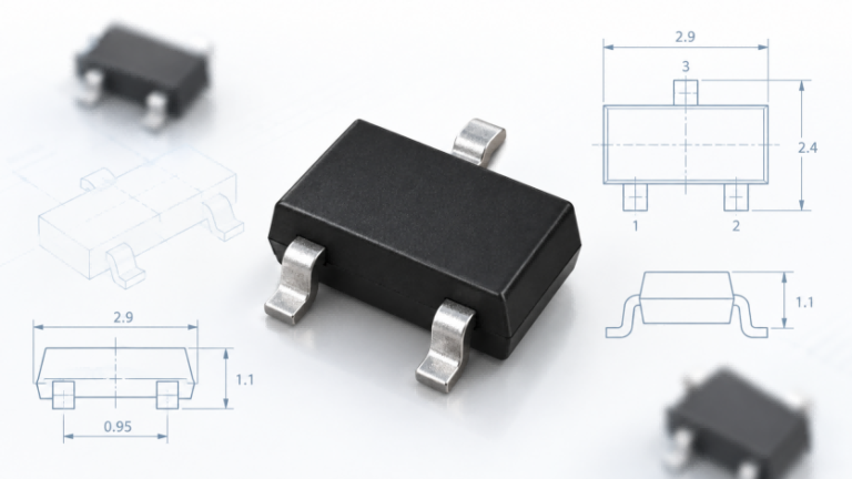
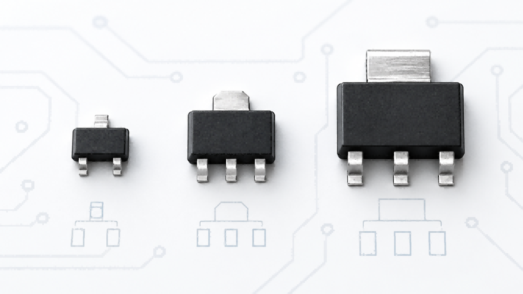
SOT-23, SOT-89, and SOT-223 are common surface-mount semiconductor packages, but they differ significantly in size, PCB footprint, and thermal performance. SOT-23 is typically used for compact, low-power circuits, SOT-89 balances space efficiency and heat dissipation, while SOT-223 offers a larger thermal connection area for applications requiring greater heat spreading.
However, package size alone does not determine power handling capability. Actual device losses, PCB copper area, and thermal requirements all influence the right choice. This guide compares the three packages and explains when to choose each one, including important considerations for component replacement.
| Feature | SOT-23 | SOT-89 | SOT-223 |
|---|---|---|---|
| Relative Size | Smallest | Medium | Largest |
| Typical Body Dimensions | 2.9 × 1.3 mm | 4.5 × 2.5 mm | 6.5 × 3.5 mm |
| Typical Terminal Configuration | 3 leads | 3 leads | 3 leads + large tab |
| PCB Footprint | Very compact | Moderate | Larger |
| Heat-Transfer Area | Limited | Wider center connection | Large thermal tab |
| Thermal Capability | Generally lower | Moderate | Generally higher with suitable PCB copper |
| Common Devices | Diodes, small-signal BJTs, MOSFETs | BJTs, regulators, switching devices | LDO regulators, power transistors |
| Main Advantage | Saves PCB space | Balances size and heat dissipation | Greater heat-spreading potential |
| Main Limitation | Limited thermal headroom | Requires additional board space | Larger PCB area requirement |
Dimensions are representative package-body measurements, excluding lead extensions. Actual package outlines and recommended PCB land patterns depend on the specific package variant and device documentation.
What Are the Differences Between SOT-23, SOT-89, and SOT-223?
SOT stands for Small Outline Transistor, a family of compact surface-mount packages originally developed for transistors but now widely used for diodes, MOSFETs, voltage regulators, and other semiconductor devices. Although SOT-23, SOT-89, and SOT-223 belong to the same broad package family, they differ substantially in physical construction and the amount of PCB space required.
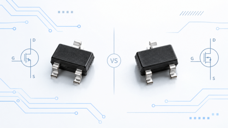
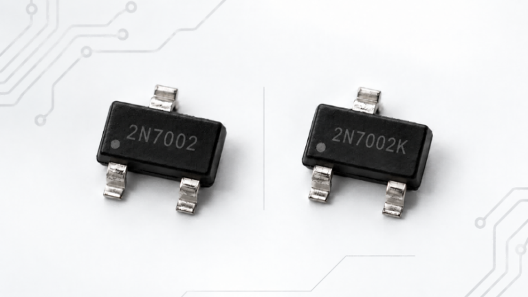
SOT-23 is the smallest of the three, with a typical three-terminal body measuring approximately 2.9 × 1.3 × 1.0 mm. Its compact dimensions make it suitable for densely populated circuit boards, especially where the component produces relatively little heat. For example, the BAS16 switching diode uses a three-lead SOT-23 package for high-speed signal switching. The BAV99 dual switching diode uses the same general package outline but contains two series-connected diodes, illustrating how different internal device configurations can share a package format.
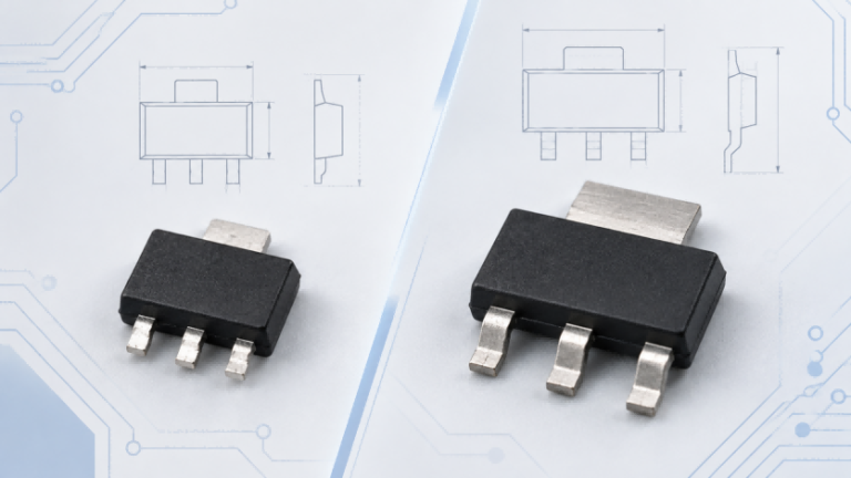
SOT-89 is larger, with a typical body measuring approximately 4.5 × 2.5 mm. Its distinctive construction includes a relatively wide center lead that provides a heat-transfer path into the PCB. Compared with SOT-23, it occupies more board space but offers greater potential for heat spreading. This makes SOT-89 an attractive option for certain medium-power transistors, voltage regulators, and switching circuits where both compactness and thermal performance matter.
SOT-223 has a typical body measuring approximately 6.5 × 3.5 mm, excluding its extended leads and prominent metal tab. The larger tab can conduct heat into a suitably designed PCB copper area, making the package useful for linear regulators and power transistors. However, the physical body size alone does not represent its complete PCB space requirement. The recommended solder pads and any additional copper reserved for heat spreading must also be considered when planning the layout.
An important distinction is that package dimensions and PCB footprints are not interchangeable measurements. The footprint includes the solder pad geometry, lead positions, and assembly clearances, while the package dimensions describe the physical component. SOT-23, SOT-89, and SOT-223 also have different terminal arrangements and land patterns. For accurate PCB design, the recommended footprint should always be checked against the specific device’s package drawing rather than selected solely by its SOT designation.
Power Dissipation and Thermal Performance
The most important functional difference between SOT-23, SOT-89, and SOT-223 is how effectively each package can transfer heat away from the semiconductor junction. Larger packages generally provide more opportunities for heat conduction into the PCB, but actual thermal performance depends on both the device construction and its mounting conditions.
This distinction becomes especially important when evaluating transistors and voltage regulators. A package may physically accommodate a device with a relatively high current rating, but that does not mean it can dissipate the resulting heat under every operating condition. Understanding power loss, thermal resistance, and PCB heat spreading is therefore essential before selecting a package for continuous operation.
Power Rating, Current Rating, and Thermal Resistance
Current rating and power dissipation describe different aspects of semiconductor operation. The current rating indicates how much current a particular device can carry under specified conditions, while power dissipation describes how much electrical energy is converted into heat. Two devices carrying the same current can produce very different amounts of heat because their internal electrical characteristics and operating conditions are different.
For example, the approximate conduction loss of a fully enhanced MOSFET can be calculated as:
P = I² × RDS(on)
For a bipolar transistor operating in saturation, the main collector-emitter conduction loss can be approximated as:
P = VCE(sat) × IC
Other losses, including switching losses, may also be significant depending on the circuit. These relationships explain why a package cannot be assigned a universal current limit independently of the device it contains. A low-resistance MOSFET carrying a relatively high current may dissipate less power than a linear regulator delivering a much smaller current.
Another important parameter is junction-to-ambient thermal resistance (θJA), usually expressed in °C/W. It describes the relationship between power dissipation and the temperature rise from the semiconductor junction to the surrounding environment under specified test conditions. A lower θJA means less junction temperature rise for the same dissipated power.
The approximate relationship is:
Temperature Rise (ΔT) = Power Dissipation (P) × Thermal Resistance (θJA)
Junction Temperature (TJ) = Ambient Temperature (TA) + ΔT
For illustration, a device dissipating 0.4 W with a junction-to-ambient thermal resistance of 150°C/W would experience an estimated junction temperature rise of 60°C. At an ambient temperature of 40°C, the estimated junction temperature would be 100°C. Whether that temperature is acceptable depends on the device’s operating limits and the required thermal margin.
SOT-23 generally has less heat-spreading capability because of its small body and limited lead contact area. SOT-89 provides a larger conductive connection to the PCB, while SOT-223 typically offers a more substantial thermal path through its metal tab. Nevertheless, there is no single thermal resistance or maximum power rating that applies to every device in a particular SOT package. The relevant values must come from the selected device’s datasheet and its stated PCB conditions.
How PCB Copper Area Affects Heat Dissipation
In surface-mount designs, the PCB plays an important role in removing heat from the semiconductor package. Heat travels from the silicon junction through the internal package structure and metal connections into the solder pads and PCB copper. Increasing the effective copper area can improve heat spreading and reduce junction temperature, particularly for packages with larger thermal connections.
This is especially relevant to SOT-89 and SOT-223. The wider center connection of SOT-89 and the large tab of SOT-223 can provide useful heat-transfer paths when attached to an appropriate copper area. However, a larger tab alone does not guarantee low thermal resistance. A SOT-223 device mounted on small, isolated pads may not achieve the same thermal performance as an identical device mounted on a properly designed copper area.
Package-level thermal comparisons demonstrate how PCB copper area affects heat dissipation. In a documented thermal evaluation using FR4 test boards, SOT-89 and SOT-223 devices exhibited different thermal resistance values with their standard mounting footprints. However, when the copper area was increased to 6 cm², both tested configurations achieved a typical junction-to-ambient thermal resistance of approximately 80°C/W. This illustrates how PCB copper layout can significantly influence thermal performance and reduce the differences between packages under certain mounting conditions.
This comparison shows why PCB copper area can matter as much as the package selection itself. Copper thickness, board layers, thermal vias, surrounding components, and airflow can also influence heat transfer. For multilayer boards, properly connected copper planes and thermal vias may improve heat spreading, although the final design should follow the device’s recommended layout and thermal guidance.
One additional consideration is that a thermal tab is not necessarily connected to ground. In some voltage regulators, for example, the tab is electrically connected to the output terminal. Connecting it to the wrong copper net can create an electrical fault regardless of how effective the thermal layout appears. The tab connection must therefore be checked in the device’s pin assignment before PCB routing.
The practical conclusion is that SOT-23, SOT-89, and SOT-223 should not be selected according to package size alone. Their thermal advantages become meaningful only when considered together with actual device losses, junction temperature limits, and the available PCB design. These factors form the basis for choosing the most suitable package for a specific circuit.
How to Choose Between SOT-23, SOT-89, and SOT-223?
Choosing the right SOT package requires balancing electrical performance, power dissipation, PCB space, and thermal requirements. Although SOT-23 is generally the most compact option and SOT-223 offers greater heat-spreading potential, neither is automatically the best choice for every circuit. The selected device must first meet the application’s electrical requirements, and its package must support reliable operation under the expected conditions.
For most designs, the decision starts with identifying suitable semiconductor devices rather than selecting a package solely by size. Once the required voltage, current, switching characteristics, and other electrical parameters are established, engineers can evaluate which available package provides sufficient thermal capability without unnecessarily increasing PCB area or assembly complexity.
Typical Applications and Package Trade-Offs
SOT-23 is commonly used in low-power signal switching, logic-level control, and compact analog circuits. Its small footprint makes it particularly useful on densely populated PCBs where thermal demands are limited. Small-signal diodes, BJTs, and MOSFETs are widely available in this package, making it a practical choice when board space is a major design constraint.
SOT-89 occupies a middle position between compact signal packages and larger power-oriented packages. Its wider center connection can help transfer heat into the PCB, making it suitable for certain medium-power switching transistors and voltage regulators. For example, the BCX56-16 transistor is an NPN device available in SOT-89 for applications requiring more substantial current capability than typical small-signal transistors.
SOT-223 is frequently found in linear voltage regulators and medium-power transistor circuits. Its large metal tab provides additional heat-spreading potential when connected to a suitable PCB copper area. The BCP56-10T1G transistor is an example of an NPN transistor supplied in SOT-223. However, its actual operating limits must be evaluated from the device specifications rather than inferred from its larger package.
The following table summarizes where each package may be considered:
| Application | Package to Consider | Main Selection Factor |
|---|---|---|
| Small-signal switching | SOT-23 | Compact size and low power loss |
| Signal processing and logic control | SOT-23 | PCB density and device availability |
| Medium-power transistor circuits | SOT-89 | Balance between footprint and thermal capability |
| Compact voltage regulators | SOT-23 / SOT-89 | Actual power dissipation and thermal limits |
| Higher-dissipation linear regulators | SOT-89 / SOT-223 | Junction temperature and PCB copper area |
| Power switching circuits | SOT-89 / SOT-223 | Device losses, current rating, and thermal design |
These are typical applications rather than fixed package assignments. A suitable SOT-89 device may outperform a particular SOT-223 device in an application if its electrical characteristics produce lower losses or better satisfy the circuit requirements. Conversely, a SOT-223 device may offer useful thermal headroom when power dissipation is a limiting factor.
For SOT-89 vs SOT-223 selection, the key question is whether the smaller package already meets the electrical and thermal requirements. If it does, SOT-89 may reduce PCB area without compromising performance. If additional heat spreading is required and sufficient copper area is available, SOT-223 may be preferable.
A Practical Package Selection Example
Consider a linear voltage regulator that converts a 12 V input to a 5 V output while supplying a continuous load current of 100 mA. Ignoring the regulator’s relatively small quiescent-current contribution, its approximate power dissipation is:
P = (VIN − VOUT) × IOUT
P = (12 V − 5 V) × 0.1 A = 0.7 W
Although the load current is only 100 mA, the regulator must continuously dissipate approximately 0.7 W as heat. This illustrates why choosing a package based solely on output current can be misleading.
Suppose two suitable regulator devices have junction-to-ambient thermal resistances of 120°C/W and 70°C/W under their respective specified PCB conditions. Their estimated junction temperature rises would be:
- At 120°C/W: 0.7 W × 120°C/W = 84°C
- At 70°C/W: 0.7 W × 70°C/W = 49°C
At an ambient temperature of 40°C, the corresponding estimated junction temperatures would be approximately 124°C and 89°C. These hypothetical values illustrate the effect of thermal resistance; they are not universal ratings for SOT-89 or SOT-223.
The final package decision depends on the regulator’s specified junction temperature limits, available PCB copper, ambient temperature, and required operating margin. A compact SOT-89 solution might be acceptable if its thermal conditions are sufficient, while another design may benefit from a SOT-223 device with a larger heat-transfer area.
For practical selection, engineers should follow a straightforward sequence: establish the required electrical characteristics, estimate power dissipation, check the device’s thermal limits, evaluate the available PCB space, and confirm the appropriate package and land pattern.
This approach helps avoid both undersized packages that may overheat and unnecessarily large packages that consume valuable PCB space.
Can SOT-23, SOT-89, and SOT-223 Replace Each Other?
SOT-23, SOT-89, and SOT-223 are generally not directly interchangeable on the same PCB footprint. Their different body dimensions, lead arrangements, pad spacing, and thermal connections mean that replacing one package with another usually requires reviewing or modifying the PCB layout. Even when two components perform the same electrical function, their package differences can prevent a direct physical replacement.
There are three important compatibility requirements to consider. Mechanical compatibility includes package dimensions, lead positions, and solder pad geometry. Electrical compatibility covers pin assignments, voltage and current ratings, switching characteristics, and other device-specific parameters. Thermal compatibility determines whether the replacement can operate within its junction temperature limits using the available PCB copper and cooling conditions.
For example, a PCB originally designed for a SOT-223 transistor may later require a replacement device available only in SOT-89. Although the smaller transistor might offer suitable electrical performance, its leads and thermal connection will not automatically align with the existing SOT-223 footprint. Temporary solder bridges or other modifications may be possible during prototype evaluation, but they should not be treated as a reliable production replacement without proper electrical, mechanical, and thermal validation.
The same caution applies when replacing devices that use an identical package outline. Two SOT-23 transistors may have different pin assignments, while two SOT-223 devices may use their large tabs for different electrical connections. Package compatibility does not guarantee electrical interchangeability.
When evaluating alternative transistors, diodes, or voltage regulators, an electronic component cross-reference search can help identify potential substitutes. Each candidate should then be checked against its datasheet for pin configuration, electrical specifications, package dimensions, and thermal requirements before approval.
Conclusion: Choosing the Right SOT Package
SOT-23, SOT-89, and SOT-223 serve different design requirements, primarily because of their physical dimensions, PCB footprint demands, and heat-transfer capabilities. SOT-23 is well suited to compact, low-power circuits, SOT-89 offers a balance between board space and thermal performance, and SOT-223 provides greater heat-spreading potential for applications requiring additional thermal capability.
The best package is not necessarily the largest one. Electrical requirements, actual power dissipation, junction temperature, and PCB layout should determine the final choice. When considering replacement components, package dimensions and pin compatibility must also be verified to ensure reliable operation.
FAQs
SOT stands for Small Outline Transistor. It refers to a family of surface-mount semiconductor packages commonly used for transistors, diodes, MOSFETs, and voltage regulators.
A common three-lead SOT-23 package has a body approximately 2.9 × 1.3 × 1.0 mm. Overall dimensions, including leads, are larger, and exact measurements depend on the package variant.
SOT-23 commonly refers to the traditional three-lead package, while SOT-23-3 explicitly indicates the three-terminal version. Other variants, including SOT-23-5 and SOT-23-6, have different lead configurations and dimensions.
No. SOT-223 packages may have different terminal configurations, mechanical tolerances, and recommended land patterns. Always verify the device-specific package drawing and PCB footprint before assuming compatibility.
Not as a direct drop-in replacement. SOT-89 and SOT-223 have different dimensions and terminal layouts. Using a SOT-89 device normally requires PCB footprint changes and verification of electrical and thermal compatibility.