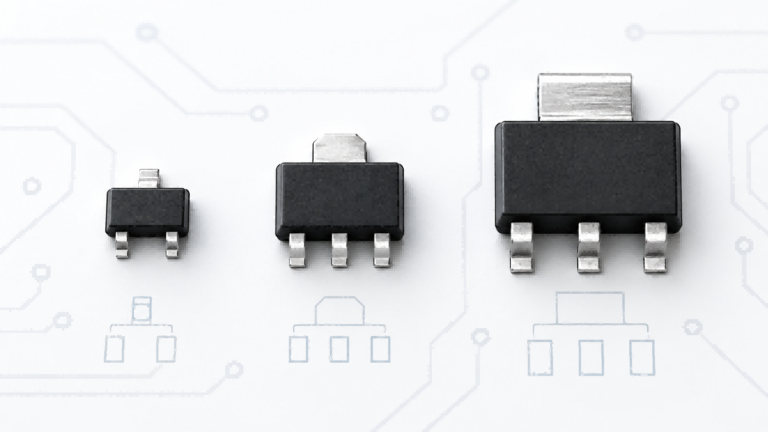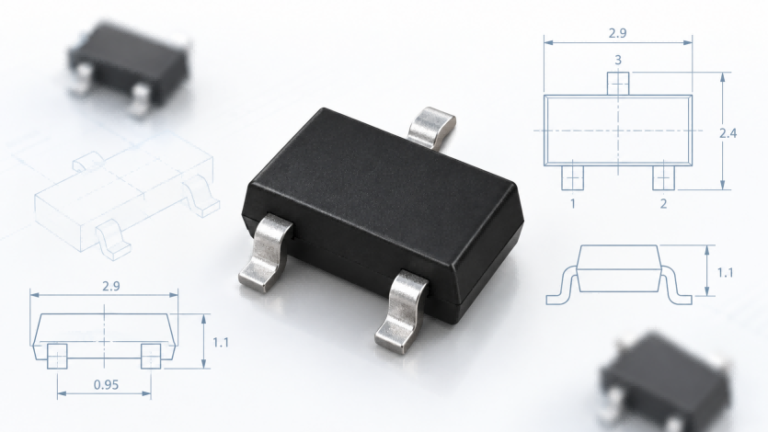
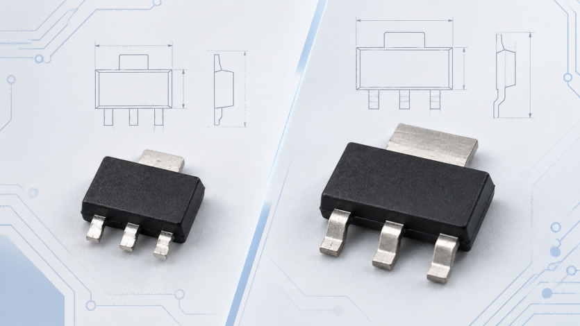
SOT-89 and SOT-223 are surface-mount packages commonly used for transistors and voltage regulators. SOT-89 is smaller and saves PCB space, while SOT-223 generally offers better heat dissipation through its larger metal tab and mounting area. However, the actual power and current ratings depend on the specific device and PCB design.
The two packages also have different footprints and are not directly interchangeable. This comparison examines their dimensions, thermal performance, and PCB compatibility to help engineers choose the right package or evaluate a potential replacement.
What Are the Differences Between SOT-89 and SOT-223?
Both SOT-89 and SOT-223 belong to the Small Outline Transistor (SOT) package family. They support surface-mount assembly and are commonly used in compact electronic circuits. Although both packages can accommodate medium-power semiconductor devices, they differ in body dimensions, terminal arrangements, PCB space requirements, and heat dissipation characteristics.
The most visible difference is that SOT-223 is physically larger than SOT-89. This additional size provides more room for heat transfer into the PCB, but it also increases the mounting area required. For engineers designing compact circuits, the choice involves balancing package size against electrical and thermal requirements.
Package Dimensions and Physical Structure
SOT-89 has a typical body size of 4.5 × 2.5 mm, while SOT-223 is larger at approximately 6.5 × 3.5 mm. Actual dimensions may vary slightly by manufacturer, so check the specific package drawing before designing the PCB footprint.
A standard three-terminal SOT-89 package has a compact rectangular body with a 1.5 mm terminal pitch. Its center terminal has a wider metal connection that can help transfer heat into the PCB. This arrangement makes SOT-89 useful in applications where board space is limited but more thermal capability is needed than a smaller signal-transistor package may provide.
SOT-223 commonly features three smaller leads on one side and a larger metal tab on the opposite side. The tab is electrically connected to an internal device terminal and provides an important path for transferring heat into the PCB. In many devices, the larger tab and one of the smaller leads are internally connected, so four physical connections do not necessarily represent four independent electrical terminals.
These structural differences affect both the mounting footprint and PCB layout. SOT-89 generally requires less board space, while SOT-223 needs larger solder pads and often benefits from additional copper connected to its metal tab.
Key Specifications at a Glance
The following table summarizes the main differences between the two common package configurations.
| Feature | SOT-89 | SOT-223 |
|---|---|---|
| Package Type | Surface-mount | Surface-mount |
| Typical Body Size | 4.5 × 2.5 mm | 6.5 × 3.5 mm |
| Terminal Arrangement | 3 terminals | 3 smaller leads + 1 large tab |
| PCB Footprint | Smaller | Larger |
| Thermal Structure | Compact metal heat-transfer connection | Larger metal tab for heat spreading |
| Power Dissipation | Device- and PCB-dependent | Device- and PCB-dependent |
| Common Components | BJTs, MOSFETs, voltage regulators | BJTs, MOSFETs, voltage regulators |
| Direct PCB Compatibility | Not directly interchangeable | Not directly interchangeable |
| Main Design Advantage | Compact mounting area | Greater heat-spreading potential |
Package references: SOT-89 (SC-62 / TO-243) and SOT-223 (SC-73). Dimensions shown are typical body measurements, not complete PCB footprint dimensions.
SOT-223 generally provides more room for heat spreading, while SOT-89 is better suited to space-constrained layouts. However, package size alone does not determine a device’s current rating, switching performance, or allowable power dissipation. These must be evaluated using the specifications of the actual component.
Thermal Performance and Power Dissipation
Thermal performance is one of the most important considerations when comparing SOT-89 and SOT-223 packages. Both can be used in circuits where transistors or regulators generate noticeable heat, but their package structures provide different opportunities for transferring that heat into the surrounding PCB.
SOT-223 generally offers better heat-spreading potential because of its larger metal tab and mounting area. SOT-89 can also dissipate heat through its metal terminals and PCB connections, but its smaller footprint typically offers less room for thermal management. Actual operating temperatures depend on the device’s thermal resistance, power dissipation, and PCB layout.
Understanding these factors is more useful than assigning a fixed power rating to either package.
Thermal Resistance and Allowable Power Dissipation
When a semiconductor operates, part of the electrical energy it processes is converted into heat. This raises the temperature of the semiconductor junction above the surrounding ambient temperature. Excessive junction temperature can reduce reliability or cause the device to exceed its operating limits.
A key parameter for evaluating thermal performance is junction-to-ambient thermal resistance (RθJA), measured in °C/W. It describes the temperature rise between the semiconductor junction and ambient air per watt of dissipated power under specified conditions. A lower value indicates more effective heat transfer in the tested thermal environment.
For steady-state operation, the approximate maximum allowable power dissipation can be calculated using:
PD,max = (TJ,max − TA) / RθJA
Where:
- PD,max: Maximum allowable power dissipation
- TJ,max: Maximum permitted junction temperature
- TA: Ambient temperature
- RθJA: Junction-to-ambient thermal resistance
For example, consider a device with a maximum junction temperature of 150°C and a thermal resistance of 100°C/W. At an ambient temperature of 50°C, the calculated steady-state power dissipation limit is approximately 1 W.
If thermal resistance decreases to 70°C/W under otherwise comparable conditions, the calculated limit increases to approximately 1.43 W. These values illustrate the relationship between thermal resistance and power dissipation; they are not fixed ratings for either package.
The calculation shows why thermal resistance matters more than package size alone. A larger package may allow better heat transfer, but the actual thermal limit also depends on the semiconductor die, internal construction, PCB design, and operating environment.
When comparing datasheets, engineers should also check how thermal resistance was measured. Two devices tested using different PCB copper areas or cooling conditions may have thermal resistance values that are not directly comparable.
PCB Copper Area and Thermal Tab Design
For many surface-mount power devices, the PCB is an important part of the heat dissipation system. Heat travels from the semiconductor junction through the package’s internal connections into the solder joints and PCB copper. It then spreads through the board before transferring to the surrounding environment.
SOT-223’s larger metal tab provides a useful thermal connection to the PCB. With an appropriately designed copper area, heat can spread across a larger region, potentially reducing the device’s operating temperature. SOT-89 also transfers heat through its metal terminals and mounting pads, although its compact footprint generally provides less area for thermal management.
The effectiveness of either package depends on the PCB layout. Copper area, copper thickness, layer structure, nearby heat sources, and airflow all influence thermal performance. In multilayer boards, properly connected copper regions and thermal vias may further improve heat spreading.
An important consideration is that the metal tab is not necessarily a ground connection. Depending on the device, it may connect to the collector, drain, output, or another electrical node. Any additional copper area must maintain the correct electrical connection and appropriate clearance from other nets.
Engineers sometimes ask whether adding more solder to a transistor’s metal terminal improves heat dissipation. Although solder conducts heat, a large solder blob cannot replace a properly designed heat-transfer path through the PCB. Its benefit depends on the connected copper area, and excessive solder can introduce assembly or reliability problems.
For both packages, the recommended approach is to use the specified land pattern and provide suitable PCB copper for the expected power dissipation.
Can SOT-89 Replace SOT-223?
SOT-89 and SOT-223 are generally not direct drop-in replacements. Their physical dimensions, terminal arrangements, and recommended PCB footprints differ. Even when two devices perform the same electrical function, they cannot automatically be exchanged without checking the existing circuit and PCB layout.
The first consideration is footprint compatibility. A PCB designed for SOT-223 typically has solder pads positioned for its three smaller leads and larger metal tab. SOT-89 uses a different land pattern, so its terminals may not align with the original pads. Having enough physical space on the board does not guarantee a reliable electrical or mechanical connection.
Pinout compatibility is equally important. For a bipolar transistor, the base, collector, and emitter must connect to the correct circuit nodes. For a MOSFET, the gate, drain, and source assignments must be verified. Voltage regulators require the same attention to input, output, ground, and other terminals. Devices with similar electrical specifications may still use different pin arrangements.
The replacement must also satisfy the original circuit’s electrical and thermal requirements. Voltage ratings, current capability, switching characteristics, safe operating area, and power dissipation should all be checked. A smaller replacement device may meet the basic electrical requirements but overheat if its package and PCB connections cannot dissipate the operating losses.
During prototyping, engineers sometimes use solder bridges or short wires to connect a smaller SOT-89 component to an existing SOT-223 footprint. Such modifications may allow limited functional testing, but they are not equivalent to a reliable production PCB design. Mechanical stability, electrical clearance, assembly consistency, and thermal performance still need to be evaluated.
When an original component becomes unavailable, an electronic component cross-reference search can help identify possible alternatives. However, matching electrical specifications alone is insufficient. Package dimensions, pin assignments, and thermal requirements must also be verified before approving a replacement.
A different package may work electrically in a redesigned circuit, but that does not make it physically compatible with the existing PCB.
Why a Smaller Package May Offer Better Device Performance
A larger semiconductor package does not necessarily contain a more capable device. Although SOT-223 generally provides greater heat-spreading potential, package size alone cannot determine switching speed, voltage ratings, current capability, or overall electrical performance. These characteristics depend on the semiconductor’s internal design and operating conditions.
This distinction becomes important when engineers discover a transistor with more suitable electrical characteristics but a smaller package. For example, a high-speed switching circuit may require low saturation voltage, suitable current gain, and short switching times. A SOT-89 transistor could meet these requirements better than a particular SOT-223 alternative, provided its electrical and thermal limits are not exceeded.
The BCX56-16 is an example of a medium-power NPN bipolar transistor available in an SOT-89 package. Its selection should depend on the circuit’s collector-emitter voltage, collector current, DC current gain, saturation voltage, and allowable power dissipation rather than package size alone.
For switching applications, engineers must also consider operating frequency, base-drive conditions, switching losses, and safe operating area. A transistor with favorable electrical specifications may still be unsuitable if its operating losses cause excessive junction temperature.
The practical lesson is that electrical performance and thermal capability should be evaluated separately. SOT-223 may provide a more favorable thermal path, but a properly selected SOT-89 device can be the better choice when its electrical characteristics and operating temperature meet the design requirements.
How Do You Choose Between SOT-89 and SOT-223?
Choosing between SOT-89 and SOT-223 requires balancing PCB space, electrical performance, thermal requirements, and component availability. Neither package is universally better. The correct choice depends on the specific semiconductor device and how it will operate in the circuit.
For compact circuits with relatively low power dissipation, SOT-89 may be the more practical option. Its smaller footprint helps conserve PCB space in transistor drivers, control circuits, and compact voltage regulation designs. However, the selected device must still satisfy the circuit’s electrical ratings and expected junction temperature.
SOT-223 becomes attractive when additional PCB space is available and greater heat spreading is desirable. For example, a linear voltage regulator with a large input-to-output voltage difference can generate substantial heat. A suitable SOT-223 regulator may provide better thermal management when its metal tab is connected to an appropriately designed copper area.
For a linear regulator with low ground-current consumption, power dissipation can be approximated as:
PD ≈ (VIN − VOUT) × IOUT
For example, a linear regulator converting 12 V to 5 V at 200 mA dissipates approximately 1.4 W. This can cause a significant temperature rise, especially when the PCB provides limited cooling. Whether a SOT-89 or SOT-223 regulator can safely handle this power depends on its thermal ratings and PCB design.
The following table summarizes how different design requirements influence package selection.
| Design Requirement | SOT-89 Consideration | SOT-223 Consideration |
|---|---|---|
| Limited PCB space | Generally preferable | Requires more mounting area |
| Low power dissipation | Often suitable | May also be suitable |
| Greater heat-spreading requirements | Requires careful thermal verification | Often provides more thermal design flexibility |
| High-speed transistor switching | Depends on device characteristics | Depends on device characteristics |
| Linear voltage regulation | Suitable within thermal limits | Useful when greater heat spreading is needed |
| Existing PCB footprint | Requires matching land pattern | Requires matching land pattern |
| Component replacement | Verify electrical and mechanical compatibility | Verify electrical and mechanical compatibility |
The BCP56-10T1G is an example of a medium-power NPN transistor in an SOT-223 package. Alongside SOT-89 devices such as the BCX56-16 discussed earlier, it illustrates why engineers must evaluate gain classification, pin configuration, power dissipation, and actual operating conditions rather than assuming that transistors with similar ratings are interchangeable.
For a new PCB design, engineers can select the package that best supports the desired device and thermal requirements. For an existing design, retaining the original footprint is often simpler unless a change in electrical performance, component availability, or thermal requirements justifies redesigning the board.
PCB Design and Component Verification Checklist
After selecting a SOT-89 or SOT-223 component, the final step is to verify that it can be mounted and operated reliably. This is especially important when changing component suppliers, evaluating alternative part numbers, or preparing a design for volume production.
Before finalizing the PCB layout and bill of materials, engineers should complete the following checks.
| Verification Item | What to Check |
|---|---|
| Exact Part Number | Complete model number, suffix, and package variant |
| Package Dimensions | Body size, terminal positions, and dimensional tolerances |
| PCB Land Pattern | Recommended solder pads, spacing, and orientation |
| Pin Configuration | Electrical terminals and metal tab connections |
| Electrical Ratings | Voltage, current, gain, switching characteristics, and operating limits |
| Thermal Requirements | Power dissipation, thermal resistance, junction temperature, and PCB copper area |
| Assembly Requirements | Soldering recommendations, placement direction, and BOM consistency |
The specific device datasheet and package drawing should determine the final design. Package names are useful for identifying the physical format, but they do not establish complete electrical or mechanical compatibility.
For production applications, any package substitution should also be validated under realistic operating conditions. A prototype that functions during a brief test may behave differently under continuous load, elevated ambient temperature, or repeated thermal cycling.
FAQs
Not as a standard drop-in replacement. SOT-89 and SOT-223 have different land patterns and terminal arrangements. Any adapted installation requires verification of electrical connections, mechanical reliability, and thermal performance.
Not necessarily. Pin assignments depend on the specific transistor, MOSFET, or regulator. Always verify the device datasheet, including the electrical connection of the metal tab.
Solder bridges may work for certain prototypes, but they are not a standard replacement method. Misalignment, mechanical stress, electrical shorts, and unreliable heat transfer can make them unsuitable for production.
Not necessarily. Solder conducts heat, but a larger solder joint does not automatically provide effective cooling. Thermal performance depends mainly on the complete heat-transfer path, including the package connections and PCB copper layout.
No. Current ratings depend on the semiconductor design and operating conditions. Although SOT-223 generally offers greater heat-spreading potential, a particular SOT-89 device may have a higher rated current than an unrelated SOT-223 device.