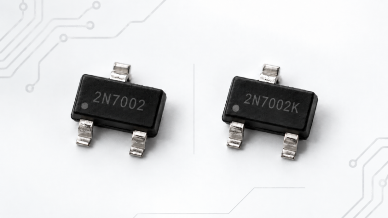
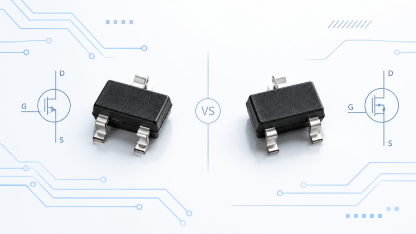
The 2N7002 and 2N7002-6AF are both 60V N-channel enhancement-mode MOSFETs in compact SOT-23 packages. They share the same basic device type, gate-source voltage rating, and pin configuration, but differ in drain current ratings, on-state resistance, and thermal characteristics.
Can 2N7002-6AF replace 2N7002? In many low-power switching circuits, it is a potential replacement. However, matching voltage ratings and package types alone does not guarantee electrical compatibility. The available gate-drive voltage, load current, conduction losses, and thermal conditions must also meet the circuit’s requirements.
This comparison uses the 2N7002 specifications from datasheet DS11303 Rev. 40-2 and the corresponding 2N7002-6AF datasheet to explain the key differences and practical replacement considerations.
What Is the Difference Between 2N7002 and 2N7002-6AF?
The 2N7002 is a widely used N-channel enhancement-mode MOSFET designed for small-signal switching, logic control, and low-power load switching. It is commonly supplied in a three-terminal SOT-23 surface-mount package. Because multiple semiconductor manufacturers produce devices under the 2N7002 designation, their electrical specifications may vary depending on the device design and test conditions.
The 2N7002-6AF is a specific version of this MOSFET family. Like the reference 2N7002, it has a 60V drain-source voltage rating, a continuous gate-source voltage rating of ±20V, and a gate threshold voltage range of 1.0V to 2.5V. Both devices also use the same basic gate, source, and drain pin arrangement. The “-6AF” suffix identifies a particular product version rather than a universally standardized performance grade.
The main differences appear in their continuous drain current, pulsed current, RDS(on), and thermal ratings. The reference 2N7002 specifies continuous drain currents of 170mA or 210mA under different PCB mounting conditions, whereas the 2N7002-6AF lists 340mA at an ambient temperature of 25°C. The 2N7002-6AF also specifies lower maximum on-state resistance values at its stated test conditions. However, higher current ratings and lower published resistance values do not automatically establish superior performance under every operating condition.
These differences matter most when replacing a component in an existing circuit. A MOSFET that fits the same PCB footprint and supports the same maximum voltage may still behave differently at a particular gate voltage or load current. Understanding the electrical characteristics is therefore essential before treating the two devices as interchangeable.
How Do 2N7002 and 2N7002-6AF Specifications Compare?
The most useful way to compare these MOSFETs is to examine their electrical ratings under the conditions specified in their datasheets. Both devices are intended for small-signal and low-power switching applications, but their published current capabilities, conduction resistance, and thermal limits are not identical.
The following comparison uses datasheet DS11303 Rev. 40-2 for the reference 2N7002 and the corresponding 2N7002-6AF product specifications. Unless otherwise specified, the values are stated at an ambient temperature of 25°C. Because the datasheets use different test currents and thermal conditions, some values should be treated as published ratings rather than results from identical laboratory tests.
2N7002 vs 2N7002-6AF Specification Comparison
| Parameter | 2N7002 | 2N7002-6AF |
|---|---|---|
| MOSFET Type | N-Channel Enhancement | N-Channel Enhancement |
| Drain-Source Voltage (VDS) | 60V | 60V |
| Gate-Source Voltage (VGS) | ±20V | ±20V |
| Continuous Drain Current (ID) | 170 / 210mA | 340mA |
| Pulsed Drain Current (IDM) | 800mA | 1.5A |
| Power Dissipation (PD) | 370 / 540mW | 350mW |
| Gate Threshold Voltage (VGS(th)) | 1.0–2.5V | 1.0–2.5V |
| RDS(on) Max @ VGS = 10V | 5.0Ω @ ID = 500mA | 2.5Ω @ ID = 300mA |
| RDS(on) Max @ Lower VGS | 7.5Ω @ 5V, 50mA | 3.0Ω @ 4.5V, 200mA |
| Thermal Resistance (RθJA) | 348 / 241°C/W | 357°C/W |
| Maximum Junction Temperature | 150°C | 150°C |
| Package | SOT-23 | SOT-23 |
| Pin Configuration | 1-G, 2-S, 3-D | 1-G, 2-S, 3-D |
| Device Marking | K72 | 7002 |
Technical references: 2N7002 datasheet DS11303 Rev. 40-2, pages 1–2; 2N7002-6AF datasheet, pages 1–2. The two continuous-current and power-dissipation values for the reference 2N7002 correspond to different PCB mounting conditions.
The table shows that both MOSFETs have the same fundamental voltage ratings and device configuration. Their most significant published differences relate to current handling and conduction resistance. However, these numbers must be interpreted alongside the specified gate voltage, drain current, and thermal conditions.
For example, the 2N7002-6AF has a higher published continuous drain current rating, but its specified maximum power dissipation is slightly lower than the 370mW rating of the reference 2N7002 under minimum-pad mounting conditions. This illustrates why continuous current and power dissipation cannot be evaluated independently.
Which Electrical Differences Matter Most?
1. Continuous Drain Current and Thermal Conditions
The reference 2N7002 specifies two continuous drain current ratings at 25°C: 170mA when mounted on an FR-4 PCB with minimum recommended pads, and 210mA when mounted on a 1 × 1-inch FR-4 board with substantial 2oz copper coverage. These ratings reflect the influence of PCB layout on heat dissipation.
The 2N7002-6AF specifies a continuous drain current of 340mA at 25°C. Although this is numerically higher, the device also has a junction-to-ambient thermal resistance of 357°C/W and a maximum power dissipation rating of 350mW. Its actual usable current depends on conduction losses, ambient temperature, PCB thermal performance, and operating conditions.
A higher maximum current rating does not mean the MOSFET can continuously carry that current in every circuit. In practical applications, engineers must ensure that the device remains within both its electrical and thermal limits.
2. RDS(on) and Conduction Losses
On-state resistance, or RDS(on), determines how much voltage is dropped across the MOSFET while it conducts current. It also influences the heat generated during switching applications.
At VGS = 10V, the reference 2N7002 specifies a maximum RDS(on) of 5.0Ω at ID = 500mA. The 2N7002-6AF specifies a maximum of 2.5Ω at ID = 300mA. At lower gate voltages, the reference device specifies 7.5Ω at VGS = 5V and ID = 50mA, while the 2N7002-6AF specifies 3.0Ω at VGS = 4.5V and ID = 200mA.
These published specifications suggest that the 2N7002-6AF can offer lower conduction resistance in relevant operating conditions. However, the test currents and gate voltages are not identical, so the values cannot be used to calculate an exact performance improvement under the same load.
For a MOSFET operating in its on-state, conduction loss can be estimated using:
Pcond ≈ ID² × RDS(on)
Likewise, the drain-source voltage drop can be estimated as:
VDS(on) ≈ ID × RDS(on)
For example, at a drain current of 100mA, an assumed on-state resistance of 5Ω produces approximately 50mW of conduction loss, while 2.5Ω produces approximately 25mW. This illustrates the relationship between resistance and power loss; it does not establish either device’s resistance at that specific operating point.
3. Gate Threshold Voltage and Drive Requirements
Both MOSFETs specify a gate threshold voltage range of 1.0V to 2.5V, measured at a drain current of 250µA. This parameter identifies the point where the MOSFET begins conducting a small specified current. It does not indicate that the device is fully enhanced or operating at its minimum resistance.
For the reference 2N7002, RDS(on) is specified at gate voltages of 5V and 10V. For the 2N7002-6AF, the specified conditions are 4.5V and 10V. Neither datasheet provides a guaranteed maximum RDS(on) at VGS = 3.3V.
Therefore, a 3.3V logic signal cannot automatically be considered sufficient for every load-switching application, even though the threshold voltage is below 3.3V. A design using 3.3V GPIO control must evaluate the required drain current, voltage drop, and switching behavior at the actual gate voltage.
For 5V-controlled circuits, the published RDS(on) specifications are more directly useful, although the difference between 5V and 4.5V test conditions should still be considered. The essential requirement is that the selected MOSFET achieves acceptable conduction performance under the circuit’s real operating conditions.
Can You Replace 2N7002 with 2N7002-6AF?
The 2N7002-6AF is a potential replacement for the reference 2N7002, but it should not be treated as an unconditional drop-in equivalent. Both devices have the same N-channel enhancement-mode configuration, 60V drain-source voltage rating, ±20V continuous gate-source voltage rating, and SOT-23 pin arrangement. These similarities make the 2N7002-6AF a reasonable candidate for substitution in many small-signal switching applications.
However, electrical compatibility depends on more than matching maximum ratings. The replacement must also provide adequate conduction performance at the available gate-drive voltage, safely handle continuous and transient load currents, and remain within the permitted junction temperature during operation.
When Is 2N7002-6AF a Suitable Replacement?
The 2N7002-6AF is most likely to be suitable when the original circuit operates comfortably within the voltage and current limits of both devices, uses a compatible SOT-23 footprint, and supplies sufficient gate voltage to achieve the required on-state resistance.
For example, a low-side switching circuit driven by a 5V logic signal and controlling a modest resistive load may be a practical candidate for replacement. Both datasheets provide on-resistance specifications near this gate-drive voltage, allowing engineers to assess the expected voltage drop and conduction loss. The final decision should also consider operating temperature, switching frequency, and the original design’s safety margins.
The following checklist provides a practical method for reviewing compatibility.
| Replacement Check | What to Verify |
|---|---|
| MOSFET Type | N-channel enhancement-mode operation matches the circuit |
| Voltage Rating | VDS and VGS ratings provide adequate operating margins |
| Gate Drive | Available VGS provides acceptable conduction performance |
| Load Current | Continuous and peak current requirements are supported |
| On-State Resistance | Voltage drop and conduction losses remain acceptable |
| Thermal Performance | Junction temperature stays within the permitted limit |
| Pinout | Gate, source, and drain match the PCB connections |
| Package | SOT-23 dimensions and footprint are compatible |
| Switching Characteristics | Dynamic performance meets circuit requirements where relevant |
For an existing PCB, matching the package and pinout is particularly important because an electrically suitable MOSFET can still be unusable if its terminal arrangement or mechanical dimensions differ. In this comparison, both devices share the same basic pin configuration, but the exact footprint and assembly requirements should still be checked.
When Should You Avoid a Direct Replacement?
A 3.3V gate-drive circuit requires additional evaluation. Both MOSFETs can begin conducting below 3.3V, but their published threshold voltages do not establish low on-state resistance at this gate voltage. If the circuit depends on a particular maximum voltage drop or must switch a relatively high load current, an unverified substitution could increase conduction losses or prevent the load from operating correctly.
Consider an example in which a microcontroller uses a 3.3V GPIO output to control a 100mA load through a low-side MOSFET switch. Before replacing the reference 2N7002 with the 2N7002-6AF, the designer should determine the maximum acceptable voltage drop and power dissipation. Because the replacement datasheet does not guarantee RDS(on) at 3.3V, its suitability at this operating point may require evaluation using characteristic curves and prototype measurements.
Higher-current applications also require caution. Although the 2N7002-6AF specifies a 340mA continuous drain current rating, it is still limited by its 350mW power dissipation rating and thermal resistance. Designs operating near current or temperature limits require a detailed thermal assessment rather than a simple comparison of maximum drain currents.
Finally, a direct replacement may be inappropriate when the original design has strict switching-speed, leakage-current, reliability, or qualification requirements. The devices have different published dynamic characteristics, measured under different test conditions. Any application that depends on these characteristics should undergo circuit-level verification before an alternate part is approved.
2N7002 and 2N7002-6AF Pinout, Package and Marking
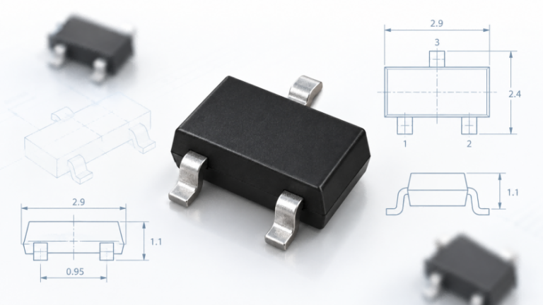
The 2N7002 and 2N7002-6AF both use a three-terminal SOT-23 surface-mount package with the same basic pin configuration. Pin 1 is the Gate (G), Pin 2 is the Source (S), and Pin 3 is the Drain (D). The gate controls channel conductivity, while the drain and source form the current path when the MOSFET is turned on. Correct pin identification is essential when checking PCB compatibility or replacing an existing component.
| Pin Number | Terminal | Function |
|---|---|---|
| 1 | Gate (G) | Controls MOSFET conduction through the gate-source voltage |
| 2 | Source (S) | Provides the reference terminal for gate-source voltage |
| 3 | Drain (D) | Connects to the load current path |
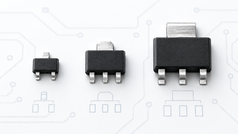
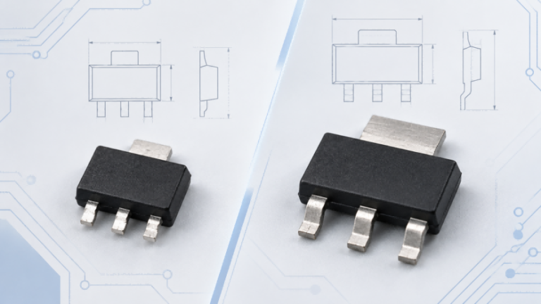
Both devices have compatible nominal SOT-23 package configurations, but the package outline and recommended PCB footprint should still be checked against the corresponding datasheets. The SOT-23 package belongs to the broader SOT package family, which includes devices with different dimensions, terminal arrangements, and thermal characteristics. Matching the package name alone is not sufficient to establish interchangeability.
Another practical difference is the device marking. The reference 2N7002 uses the marking K72, while the 2N7002-6AF uses 7002. These markings can help identify components on an assembled PCB, although other manufacturers may use different marking codes for similar devices. The complete part number and supplier documentation remain necessary for reliable identification.
Typical Applications of 2N7002 and 2N7002-6AF
The 2N7002 and 2N7002-6AF are commonly suited to small-signal switching and low-power electronic control circuits. Their compact SOT-23 packages make them useful in space-constrained designs, while their voltage-controlled gates allow them to interface with digital control circuitry. Typical applications include signal switching, low-current load control, logic interfacing, and general-purpose switching functions.
In low-side load-switching circuits, the MOSFET is placed between the load and ground, with the gate driven by a control signal. When sufficient gate-source voltage is applied, the MOSFET conducts and allows current to flow through the load. For applications such as indicator control or small electronic loads, the most important selection factors are the available gate voltage, load current, RDS(on), and thermal performance. A low gate threshold voltage alone does not establish whether either device can efficiently drive a particular load.
Both MOSFETs may also be considered for logic-level translation circuits, depending on the circuit topology and signal requirements. For example, an N-channel MOSFET can be used in certain bidirectional open-drain level-shifting circuits with suitable pull-up resistors. Unlike load switching, these applications place greater emphasis on signal voltage levels, leakage current, capacitance, and switching behavior. The actual circuit configuration determines whether either MOSFET is appropriate.
What Are the Alternatives to the 2N7002 MOSFET?
Several N-channel MOSFETs can serve as alternatives to the 2N7002, but they are not necessarily direct replacements. An electrically similar MOSFET may perform the same switching function while using a different package, pin configuration, voltage rating, or on-state resistance. Therefore, it is important to distinguish between a functional equivalent and a drop-in replacement that can be installed in an existing circuit without modifications.
The following devices are commonly considered when evaluating alternatives to the 2N7002.
| Alternative MOSFET | Package | Key Considerations |
|---|---|---|
| BSS138 | SOT-23 | N-channel MOSFET; compare voltage rating, current capability, RDS(on), and pinout |
| 2N7000 | TO-92 | Similar general-purpose switching function, but uses a through-hole package |
| AO3400A | SOT-23 | Low-voltage N-channel MOSFET with different voltage and current characteristics; not suitable for all 60V applications |
The BSS138 is a possible alternative in certain small-signal applications, but its electrical characteristics must be checked against the original circuit requirements. The 2N7000 provides a comparable general-purpose switching function in a TO-92 through-hole package, making it more suitable for designs that allow a package change. The AO3400A offers different conduction and current-handling characteristics, but its lower drain-source voltage rating makes it unsuitable for applications that require the full 60V capability of the 2N7002.
When selecting replacement MOSFETs for an existing PCB or bill of materials, begin with the required voltage rating, gate-drive conditions, load current, and physical compatibility. A cross-reference search can help identify additional candidate components, but final approval should be based on the corresponding datasheets and actual circuit requirements.
Conclusion
The 2N7002 and 2N7002-6AF share the same fundamental N-channel MOSFET configuration, 60V drain-source voltage rating, and SOT-23 pin arrangement. However, they differ in continuous drain current ratings, published on-state resistance, and thermal characteristics.
The 2N7002-6AF is a potential replacement for the 2N7002, but compatibility must be verified under actual operating conditions. Gate-drive voltage, load current, conduction losses, thermal limits, and PCB compatibility should guide the final decision. For projects requiring component sourcing or alternative-part evaluation, CNCHIPDEPOT provides electronic component sourcing support.
FAQs
The BSS138, 2N7000, and AO3400A are potential alternatives for certain applications. However, they differ in voltage ratings, electrical characteristics, or package types. A direct replacement must satisfy the original circuit’s voltage, current, gate-drive, and pinout requirements.
The reference 2N7002 is a 60V N-channel enhancement-mode MOSFET in a SOT-23 package. It has a ±20V continuous gate-source rating, a 1.0–2.5V gate threshold range, and continuous drain current ratings of 170mA or 210mA under specified PCB mounting conditions.
A 2N7002 may work with 3.3V logic in certain low-current circuits, but compatibility is not guaranteed. Its gate threshold voltage does not indicate full enhancement. Check the required drain current, acceptable voltage drop, and on-state resistance at the actual gate-drive voltage.
They can be interchangeable in applications where their electrical and thermal characteristics satisfy the same circuit requirements. Both have 60V ratings and compatible SOT-23 pin arrangements, but differences in RDS(on), current ratings, and operating conditions must be evaluated before replacement.
The main difference is the package. The 2N7000 typically uses a TO-92 through-hole package, while the 2N7002 uses a SOT-23 surface-mount package. Their electrical specifications can also differ, so they should not be treated as PCB-compatible replacements without verification.