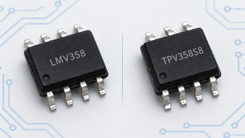
The LMV358 and TPV358S8 are low-voltage dual operational amplifiers commonly considered for analog signal conditioning, sensor interfaces, and battery-powered electronics. Both offer a 1 MHz gain-bandwidth product and rail-to-rail output capability, but they differ in input architecture, power consumption, slew rate, and supply voltage requirements.
Can TPV358S8 replace LMV358? It can be considered a potential alternative when the pinout, package dimensions, supply voltage, input range, and output performance meet the original circuit requirements. However, similar specifications do not guarantee a direct replacement.
This guide compares their electrical characteristics, explains the main compatibility considerations, and provides practical guidance for selecting and evaluating these operational amplifiers.
What Are LMV358 and TPV358S8?
The LMV358 is a low-voltage, dual-channel operational amplifier with rail-to-rail output (RRO) capability. It contains two independent amplifiers in a single integrated circuit and operates from a 2.7V to 5.5V supply. With a typical gain-bandwidth product of 1 MHz, it is suitable for general-purpose amplification, sensor signal conditioning, and other low-voltage analog circuits.
The TPV358S8 is a low-power CMOS dual operational amplifier designed for single-supply operation from 2.2V to 5.5V. Unlike the LMV358, it features rail-to-rail input and output (RRIO) capability, allowing operation with input signals closer to both supply rails. It also incorporates RF interference suppression and has a typical total quiescent current of approximately 80 µA. The TPV358S8 uses an SOP-8 package.
Although both devices perform similar amplification functions, they are not identical. Their different input architectures, power consumption, and dynamic characteristics can influence performance in specific circuits. Understanding these differences is important before considering one as a replacement for the other.
What Are the Key Differences Between LMV358 and TPV358S8?
The main differences between LMV358 and TPV358S8 involve their input voltage range, current consumption, signal speed, and input characteristics. Both provide two amplifier channels and a typical 1 MHz gain-bandwidth product, but their electrical behavior differs under certain operating conditions.
Electrical Specifications Comparison
The following table compares the electrical specifications most relevant to component selection and replacement.
| Parameter | LMV358 | TPV358S8 |
|---|---|---|
| Amplifier Type | Dual operational amplifier | Dual operational amplifier |
| Input Architecture | Bipolar | CMOS |
| Supply Voltage | 2.7–5.5V | 2.2–5.5V |
| Rail-to-Rail Capability | Rail-to-Rail Output | Rail-to-Rail Input and Output |
| Gain-Bandwidth Product (Typ.) | 1 MHz | 1 MHz |
| Slew Rate (Typ.) | 1 V/µs | 0.6 V/µs |
| Quiescent Current (Typ., Total) | 210 µA | 80 µA |
| Input Offset Voltage (Max.) | 7 mV | 5 mV |
| Input Bias Current | 250 nA max. | 10 pA typ. |
| Operating Temperature | −40°C to +125°C | −40°C to +125°C |
| RF Filtering | Not listed as an integrated feature | Integrated anti-RF filter |
| Package | SOIC-8, TSSOP-8, VSSOP-8 | SOP-8 |
The values above are based on the respective LMV358 and TPV358 series technical specifications. Typical and maximum values represent different test conditions and should not be interpreted as directly equivalent limits.
The TPV358S8 operates at a lower minimum supply voltage and draws less typical quiescent current. Its CMOS input architecture also provides lower input bias current, which can be advantageous in high-impedance sensor circuits. In contrast, the LMV358 offers a higher typical slew rate, making it potentially better suited to signals that require faster output voltage transitions.
Despite having the same nominal 1 MHz gain-bandwidth product, the two devices should not be assumed to deliver identical performance. Input range, output loading, signal amplitude, and amplifier stability can all influence how they behave in an actual circuit.
Rail-to-Rail Input and Output Differences
One of the most important distinctions is the difference between rail-to-rail output (RRO) and rail-to-rail input/output (RRIO).
The LMV358 provides rail-to-rail output operation, but its input common-mode voltage range does not extend fully to the positive supply rail. It can accommodate input voltages around the negative supply rail, making it useful for ground-referenced signals. However, an input approaching the positive supply may exceed its specified common-mode operating range.
The TPV358S8 provides rail-to-rail input and output operation, allowing it to handle input signals closer to both supply rails. This can be useful in low-voltage sensor circuits where the input signal occupies a large portion of the available supply range.
For example, consider a sensor amplifier powered by 3.3V with an input signal approaching 3.2V. The LMV358 may not accommodate this input level within its specified common-mode range, even though 3.3V is a valid supply voltage. The TPV358S8 offers a wider input range, although its exact operating limits must still be checked.
Rail-to-rail output also does not guarantee that the amplifier can produce an output exactly equal to the supply voltage. Actual output swing depends on output current, load resistance, and operating conditions. Heavier loads generally increase the voltage headroom required near the supply rails.
Power Consumption, Speed, and Signal Accuracy
The differences in power consumption, speed, and input characteristics can affect which amplifier is better suited to a particular application.
| Characteristic | LMV358 | TPV358S8 | Practical Impact |
|---|---|---|---|
| Quiescent Current | 210 µA typ. | 80 µA typ. | TPV358S8 may reduce idle power consumption |
| Slew Rate | 1 V/µs | 0.6 V/µs | LMV358 supports faster typical output transitions |
| Input Bias Current | Higher | Lower | TPV358S8 may reduce errors with high-impedance sources |
| Input Voltage Range | Includes negative rail | Rail-to-rail input | TPV358S8 accommodates a wider input range |
| Input Offset Voltage | 7 mV max. | 5 mV max. | Lower specified offset may benefit DC accuracy |
| RF Immunity Feature | No integrated filter specified | Anti-RF filtering | TPV358S8 includes an additional interference suppression feature |
Power consumption is a notable difference. The TPV358S8 has a typical total quiescent current of 80 µA, compared with 210 µA for the LMV358. This may benefit battery-powered instruments and continuously operating monitoring circuits. However, quiescent current does not include all current delivered to external loads, so total system power consumption depends on the actual circuit.
Signal speed presents a different trade-off. Although both amplifiers have a typical 1 MHz gain-bandwidth product, the LMV358 has a higher typical slew rate. This can matter when amplifying large-amplitude or rapidly changing signals, where an insufficient slew rate may cause distortion.
Input accuracy also deserves consideration. The TPV358S8’s low input bias current can reduce voltage errors caused by current flowing through high source resistance. Its lower specified maximum offset voltage may also be useful in some DC measurement applications, although noise, temperature drift, and actual operating conditions must be considered.
The TPV358S8 additionally integrates RF interference suppression, which may improve immunity to unwanted high-frequency signals. Nevertheless, this feature does not replace proper PCB layout, grounding, and power-supply decoupling.
Neither device is universally superior. The TPV358S8 offers advantages in low-power operation and high-impedance inputs, while the LMV358 provides a higher typical slew rate. The better choice depends on the requirements of the intended circuit.
Can TPV358S8 Replace LMV358?
TPV358S8 may replace LMV358 in electrically and mechanically compatible circuits, especially where low-voltage operation and modest signal bandwidth are required. However, the substitution should not be treated as automatically interchangeable simply because both devices contain two operational amplifiers and share a 1 MHz gain-bandwidth specification.
Replacement suitability depends on matching the pin configuration and package dimensions, as well as meeting the original circuit’s supply voltage, input range, output drive, stability, and accuracy requirements.
Pinout and Package Compatibility
The LMV358 and TPV358S8 use the conventional eight-pin dual operational amplifier pin configuration in their corresponding SOIC-8 and SOP-8 versions. Each contains two amplifier channels with separate inputs and outputs and shared power-supply connections.
| Pin Number | Pin Function | Description |
|---|---|---|
| 1 | OUT A | Amplifier A output |
| 2 | IN− A | Amplifier A inverting input |
| 3 | IN+ A | Amplifier A non-inverting input |
| 4 | V− | Negative supply or ground |
| 5 | IN+ B | Amplifier B non-inverting input |
| 6 | IN− B | Amplifier B inverting input |
| 7 | OUT B | Amplifier B output |
| 8 | V+ | Positive supply |
The corresponding eight-pin configurations use matching electrical pin functions. However, the exact ordering codes and package drawings should be checked before replacement. LMV358 devices are available in multiple packages, and not every package version fits the same PCB footprint.
Pin-compatible does not automatically mean drop-in compatible. Even if the electrical connections match, differences in body dimensions, lead pitch, or recommended solder-pad layout may prevent direct installation. The package outline and pin-1 orientation should therefore be verified for the actual devices being used.
When Replacement Is Possible—and When It Requires Caution
The following table summarizes common circuit conditions and the associated replacement considerations.
| Circuit Condition | Replacement Consideration | Recommendation |
|---|---|---|
| 3.3V or 5V supply | Both devices support these voltages | Potential candidate; verify other requirements |
| Low-frequency sensor amplification | Similar general-purpose amplification capabilities | Replacement may be possible |
| Input near positive supply rail | Different input common-mode ranges | Check input limits carefully |
| Fast-changing signals | Different slew rates | Verify dynamic performance |
| High-impedance sensors | Different input bias currents | Evaluate measurement errors |
| Higher output loads | Output-drive capabilities may differ | Check output current and voltage swing |
| Precision analog circuits | Offset, noise, and drift can affect accuracy | Perform application-level validation |
| Capacitive output loads | Stability characteristics may differ | Verify stability in the original circuit |
For low-frequency sensor amplifiers and general-purpose signal-conditioning circuits, the TPV358S8 may be an appropriate replacement candidate when the operating conditions fall within its specifications. Its lower input bias current and wider input range may even offer advantages in certain designs.
Greater caution is necessary when the original circuit requires fast signal transitions, substantial output drive, or precise analog measurements. The TPV358S8’s lower typical slew rate can affect large-signal response, while differences in output characteristics and noise may influence circuit performance.
A replacement may also require additional testing when the amplifier drives a capacitive load or operates in a feedback configuration sensitive to changes in device characteristics. Matching the nominal bandwidth alone is not sufficient to establish equivalent stability or transient response.
Replacement Verification Checklist
Before replacing LMV358 with TPV358S8, engineers should compare the device specifications against the actual circuit requirements.
| Verification Item | What to Check |
|---|---|
| Pin Configuration | Confirm all eight pin functions match |
| Package Dimensions | Compare lead pitch, body dimensions, and PCB footprint |
| Supply Voltage | Verify the full operating supply range |
| Input Common-Mode Range | Confirm all expected input voltages are supported |
| Output Voltage Swing | Verify the required output voltage under load |
| Output Drive | Check load current and output capability |
| GBW and Slew Rate | Confirm bandwidth and signal transition requirements |
| Offset and Noise | Evaluate accuracy and signal quality |
| Temperature Range | Check operating limits and parameter variation |
| Stability | Evaluate feedback and capacitive-load behavior |
A practical verification process begins with comparing electrical specifications and mechanical drawings. After confirming pin and package compatibility, the candidate amplifier should be evaluated in the actual circuit under representative supply voltages, signal conditions, output loads, and operating temperatures.
For additional component alternatives, a cross-reference search can help identify potential replacement part numbers for further evaluation. Cross-reference results should always be verified against the relevant electrical and mechanical specifications before substitution.
LMV358 and TPV358S8 in Practical Applications
The differences between LMV358 and TPV358S8 become more meaningful when considered in actual circuit applications. Both devices can be used for general-purpose analog amplification, but their suitability depends on the signal characteristics, power requirements, and connected components.
| Application | Key Requirement | Selection Consideration |
|---|---|---|
| Sensor Signal Conditioning | Input common-mode range | TPV358S8 offers rail-to-rail input capability |
| Battery-Powered Instruments | Low current consumption | TPV358S8 has lower typical quiescent current |
| High-Impedance Sensor Interfaces | Low input bias current | TPV358S8 may reduce bias-current-related errors |
| Faster Analog Signals | Slew rate | LMV358 has a higher typical slew rate |
| General Analog Buffers | Output swing and load capability | Evaluate both devices under actual load conditions |
| RF-Exposed Sensor Circuits | Interference immunity | TPV358S8 includes integrated anti-RF filtering |
In low-voltage sensor amplification, input common-mode range is often an important selection factor. For example, a 3.3V-powered sensor may produce a signal that approaches the positive supply rail. The LMV358 may not accommodate the entire signal range within its specified input limits, while the TPV358S8’s rail-to-rail input design may provide greater flexibility.
For battery-powered equipment, reducing continuous current consumption can help extend operating time. The TPV358S8’s lower typical quiescent current may therefore be useful in portable measuring instruments and monitoring systems. The actual benefit depends on the total system power budget and whether the amplifier operates continuously or intermittently.
In high-impedance sensor interfaces, input bias current may be more important than small differences in bandwidth. Photodiode amplifiers, resistive sensors, and other high-impedance signal sources can develop measurement errors when amplifier bias current flows through the source resistance. The TPV358S8’s low typical input bias current may reduce this effect, although circuit noise, offset voltage, and stability must also be considered.
The appropriate device should be selected according to the application’s most demanding electrical conditions. A lower-power amplifier may be advantageous for slow sensor signals, while a higher slew rate may be more useful for rapidly changing waveforms.
LMV358, LM358, and LMV358A: Related Alternatives
The LMV358, LM358, and LMV358A are all dual operational amplifiers, but they have different electrical characteristics and should not be treated as identical components.
| Device | Main Characteristics | Replacement Consideration |
|---|---|---|
| LMV358 | Low-voltage, 1 MHz, rail-to-rail output | Reference device for comparison |
| LM358 | General-purpose dual op amp, wider supply range | Different output characteristics and voltage requirements |
| LMV358A | Improved LMV358 variant with lower offset and faster slew rate | Upgraded replacement for corresponding LMV358 configurations |
| TPV358S8 | Low-power CMOS, 1 MHz, rail-to-rail input/output | Candidate alternative requiring compatibility verification |
The LM358 supports a different operating voltage range and does not provide the same rail-to-rail output behavior as the LMV358. Although their names and basic functions are similar, they should not be substituted without reviewing the circuit requirements.
The LMV358A is an upgraded alternative to the LMV358, offering improvements such as a typical 1.7 V/µs slew rate, a maximum input offset voltage of 4 mV, and lower quiescent current. It is identified as a drop-in upgrade for corresponding LMV358 configurations, subject to selecting the appropriate package and ordering code.
The TPV358S8 remains a separate low-power alternative. Its CMOS architecture and rail-to-rail input capability provide different advantages, but direct replacement should be determined through electrical and mechanical compatibility checks rather than part-number similarity.
Conclusion
The LMV358 and TPV358S8 are similar low-voltage dual operational amplifiers, but their differences in input architecture, power consumption, and slew rate can influence circuit performance. The TPV358S8 offers lower typical quiescent current and rail-to-rail input capability, while the LMV358 provides a higher typical slew rate.
TPV358S8 may replace LMV358 when the electrical and mechanical requirements are compatible, but each substitution should be confirmed through specification comparison and circuit-level validation. For electronic component sourcing and replacement requirements, CNCHIPDEPOT provides component selection and alternative sourcing support.
FAQs
Yes. The LMV358 operates from 2.7V to 5.5V, so both 3.3V and 5V are within its specified supply range. Input common-mode and output swing limits still apply.
Yes, but only its output is rail-to-rail. The LMV358 is an RRO operational amplifier, not a full RRIO device. Its input range does not extend fully to the positive supply rail.
Rail-to-rail output still requires voltage headroom. The LMV358’s output swing depends on load resistance, output current, and supply conditions. Heavier loads can prevent the output from approaching the supply rails closely.
No. The LMV358 is designed for low-voltage operation with rail-to-rail output capability. Conventional LM358 devices have different supply voltage and output swing characteristics, so they are not automatically interchangeable.
Yes. The TPV358S8 has a typical total quiescent current of 80 µA, compared with approximately 210 µA for the LMV358. Actual circuit power consumption also depends on supply voltage, output loading, and operating conditions.