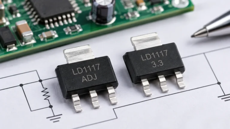
The LD1117-3.3 and LD1117-5.0 are fixed-output low-dropout linear regulators from the same LD1117 family. The most obvious difference is their output voltage: one regulates to 3.3V and the other to 5.0V. That difference also changes how much input-voltage headroom each version needs and how much heat it must dissipate in the same circuit.
For most designs, the choice starts with the load: use the 3.3V version for a 3.3V supply rail and the 5.0V version for a 5V rail. Before finalizing the choice, however, you also need to check input voltage, dropout margin, load current, and power dissipation. In some high-voltage or high-current conditions, neither version may be the best regulator for the job.
What Is the Difference Between LD1117-3.3 and LD1117-5.0?
Both versions perform the same basic function: they take a higher DC input voltage and regulate it down to a fixed lower voltage. The key electrical difference is therefore not their basic regulator architecture, but the output rail they are designed to maintain.
That output-voltage difference has practical consequences. A 3.3V regulator can operate from a lower input supply than a 5V regulator because the latter must maintain a higher output while still preserving enough voltage across the regulator to remain in regulation. At the same input voltage and load current, the 3.3V version also drops more voltage and therefore dissipates more power as heat.
Quick Comparison
| Parameter | LD1117-3.3 | LD1117-5.0 | Practical Meaning |
|---|---|---|---|
| Fixed output voltage | 3.3V | 5.0V | Must match the required supply rail |
| Output current capability | Up to 800mA* | Up to 800mA* | Actual continuous current can be thermally limited |
| Typical dropout behavior | Similar | Similar | The 5V version still needs a higher Vin because its Vout is higher |
| Full-load characterization Vin | 4.75V | 6.5V | Useful reference conditions, not universal minimum-input limits |
| Quiescent current | Same family behavior | Same family behavior | Usually not the main reason to choose between them |
| Protection | Current and thermal limiting | Current and thermal limiting | Shared protection behavior |
*The current LD1117 production datasheet specifies up to 800mA output current, 1V typical dropout, internal current and thermal limiting, and fixed 3.3V and 5.0V options. It also specifies output-voltage tolerance within ±1% at 25°C for the relevant grade.
One important qualification is that the name “LD1117” is also used across second-source or compatible products whose published specifications are not always identical. A product carrying a similar part designation may advertise different current, maximum input voltage, or dropout limits. For production design, the datasheet for the exact device being purchased should therefore override a generic 1117-family specification.
Why Does the Output Voltage Difference Matter?
The regulator should be selected from the load requirement backward. If a microcontroller, sensor, memory device, or other circuit requires a 3.3V supply, choosing a 5V regulator simply because it provides a higher voltage would be incorrect and could exceed the load’s allowed supply voltage. Likewise, a circuit designed around a 5V rail normally needs the 5V version rather than a 3.3V substitute.
The difference also affects voltage headroom. A linear regulator cannot produce its rated output when the input is only equal to the required output voltage. It needs some additional voltage across the device—its dropout margin—to maintain regulation. That is why a 5V supply can be a practical input for LD1117-3.3, while the same 5V supply cannot be used to obtain a properly regulated 5V output from LD1117-5.0.
Finally, the lower output voltage does not mean the 3.3V version is automatically the more efficient choice. If both versions operate from the same Vin and deliver the same current, the 3.3V regulator has to remove a larger voltage difference. That additional voltage is converted into heat rather than useful output power.
How Do You Choose Between LD1117-3.3 and LD1117-5.0?
The most reliable selection process is to answer two questions in order. First, does the input voltage provide enough headroom for regulation? Second, once it does, can the regulator dissipate the resulting heat at the required load current?
This order matters because an input voltage can fail in two opposite ways. If it is too close to Vout, the regulator falls into dropout and can no longer hold the specified output voltage. If it is much higher than Vout, regulation may be electrically possible but power dissipation can become excessive.
Check Output Voltage and Input Headroom First
Start with the load’s required voltage. If the rail must be 3.3V, the relevant fixed-output device is LD1117-3.3. If the rail must be 5V, start with LD1117-5.0. Once the output requirement is fixed, compare the available Vin with the regulator’s dropout requirement.
A useful first approximation is:
Vin(min) ≈ Vout + Vdropout
However, dropout should not be treated as one fixed number under every operating condition. In the current LD1117 electrical characteristics, the standard device is specified at about 1.0V typical / 1.1V maximum at 100mA, 1.05V typical / 1.15V maximum at 500mA, and 1.10V typical / 1.20V maximum at 800mA under the stated temperature conditions.
For a reader choosing a regulator, the practical interpretation is straightforward: higher load current can require slightly more input-voltage margin. A design that appears comfortable at 100mA should not automatically be assumed to have the same margin at 800mA.
| Available Input | LD1117-3.3 | LD1117-5.0 | Practical Judgment |
|---|---|---|---|
| 5V | Commonly suitable if adequate margin remains under load | Cannot provide a properly regulated 5V output | Natural case for 5V → 3.3V conversion |
| Around 6V | Good headroom for 3.3V | Can be marginal at heavier loads | Check dropout under the actual current |
| 7–9V | Electrically possible | Electrically possible | Thermal loss becomes increasingly important |
| 12V | Electrically possible within the device input range | Electrically possible within the device input range | Do not judge suitability from voltage limit alone |
The production datasheet characterizes the 3.3V version across a 0–800mA load range with 4.75V input for load-regulation testing, while the corresponding 5V version uses a higher input condition. These are useful design-reference conditions, but they should not be interpreted as universal hard minimum Vin values for every load and temperature.
This distinction becomes particularly important with sources that sag under load. A nominal 5V rail may be adequate for LD1117-3.3, but cable resistance, connector loss, battery discharge, or upstream supply tolerance can reduce the voltage actually reaching the regulator. The correct question is therefore not just “Is my supply labeled 5V?” but “What is the lowest Vin at the regulator under the worst expected load?”
Then Check Load Current and Heat
Once sufficient input headroom has been confirmed, the next question is whether the regulator can handle the voltage drop at the required current. For a linear regulator, a useful approximation for regulator power loss is:
Pd ≈ (Vin − Vout) × Iout
Consider a 9V input and a 300mA load. With LD1117-3.3:
Pd ≈ (9 − 3.3) × 0.3 = 1.71W
With LD1117-5.0:
Pd ≈ (9 − 5.0) × 0.3 = 1.20W
Both regulators may have enough input-voltage headroom, but the 3.3V version must dissipate about 0.51W more heat under the same input and load conditions. This is why “Vin is within the allowed range” is not enough to determine whether a linear regulator is practical.
The same reasoning explains why the published 800mA output capability should not be read as “800mA continuous under any condition.” How much continuous current a finished board can sustain also depends on package thermal resistance, PCB copper area, ambient temperature, airflow, and the size of Vin−Vout. The datasheet itself provides different thermal-resistance values for different packages, reinforcing that thermal capability is tied to the physical design rather than current rating alone.
For an initial selection, the process can therefore be kept simple:
- Determine whether the load requires 3.3V or 5V.
- Check that the lowest expected Vin leaves adequate dropout margin.
- Calculate approximate power loss using
(Vin − Vout) × Iout. - Check whether the package and PCB can dissipate that power without exceeding the allowable junction temperature.
- If the voltage drop or thermal loss is excessive, reconsider the regulator choice rather than assuming a larger heatsink will always solve the problem.
This approach avoids two common mistakes: choosing the correct output voltage but not leaving enough input margin, or providing plenty of input voltage while overlooking the heat generated by dropping the excess voltage.
Can LD1117-3.3 and LD1117-5.0 Be Interchanged?
The two fixed-output versions may share the same package and pin arrangement, but that does not make them functionally interchangeable. Package compatibility, pin compatibility, and electrical compatibility are different things. A regulator can fit the same PCB footprint and still be unsuitable because its output voltage does not match the circuit it is powering.
For example, replacing a 3.3V regulator with a 5.0V version can expose downstream components to a voltage they were never designed to tolerate. The reverse substitution may not damage a 5V load, but the lower voltage can prevent the circuit from operating correctly. Before replacing one version with the other, the output rail requirement must therefore be checked first.
| Compatibility Check | What to Verify |
|---|---|
| Package | Does the replacement fit the same footprint? |
| Pinout | Are VIN, VOUT, GND, and the tab arranged the same way? |
| Output voltage | Does the load require 3.3V or 5V? |
| Current capability | Can the exact device support the required load? |
| Thermal conditions | Will Vin−Vout create acceptable power dissipation? |
| Capacitors | Does the exact device use compatible stability requirements? |
For fixed-output LD1117 variants in the same package, the pin arrangement may be the same, but the output-voltage suffix is still a functional specification, not just a naming difference. If an existing board needs a replacement, the safest approach is to verify the full part number, output voltage, package, current rating, and datasheet conditions rather than assuming every 1117-family device is a drop-in substitute.
For broader replacement work, an electronic parts cross reference can help identify possible alternatives, but any candidate still needs datasheet-level validation before it is treated as electrically compatible.
Capacitor and Stability Requirements
The external capacitors around an LD1117 are not optional details. They help the regulator remain stable and respond correctly when the load changes. For the current LD1117 documentation used as the primary technical reference here, a minimum 10µF output capacitor is specified for stability, while the standard fixed-output application circuit also includes local input decoupling.
This does not mean that every regulator carrying a similar 1117 designation has identical capacitor requirements. Second-source parts and related 1117-family devices can differ in their recommended capacitance, ESR range, and ceramic-capacitor behavior. That is why capacitor recommendations from one device should not automatically be copied to another simply because the package and pinout look similar.
For most readers, the practical rule is simple: use the capacitor values and conditions specified for the exact device being installed, and place the capacitors close to the regulator rather than treating them as generic board-level components. If a design is being converted from one 1117-family source to another, capacitor compatibility should be checked along with output voltage and pinout.
When Is LD1117 Not the Best Choice?
The LD1117 remains useful in many simple linear-regulator designs, particularly when the input-to-output voltage difference is modest and the required current can be handled without excessive heat. It can also make sense in an existing design that is already validated and does not have a strong efficiency or battery-life requirement.
However, another regulator architecture may be more appropriate when:
- the input voltage is much higher than the required output voltage;
- continuous load current produces excessive power dissipation;
- battery life is an important design target;
- the enclosure has limited airflow or PCB area for heat spreading;
- very low quiescent current or significantly lower dropout is required.
The important point is not that LD1117 is inherently unsuitable for new designs. The better question is whether its electrical and thermal characteristics match the application. A familiar part should not be selected automatically if the required voltage drop, current, or efficiency makes the design difficult to cool.
When the linear-regulator approach is no longer a good fit, other power management ICs can be compared based on input range, output current, efficiency, package, and thermal limits rather than forcing either LD1117 version into an unsuitable operating condition.
Which One Should You Choose?
Choose LD1117-3.3 when the load requires a regulated 3.3V rail, the available input voltage stays high enough above 3.3V under load, and the resulting power dissipation can be managed by the package and PCB.
Choose LD1117-5.0 when the load requires 5V and the input remains sufficiently above 5V to maintain regulation. As with the 3.3V version, the available current is not determined by the headline current rating alone; thermal conditions still matter.
The selection can be reduced to one practical rule: match the regulator to the load voltage first, then confirm input headroom and thermal feasibility. If either version would operate too close to dropout or dissipate too much heat, the correct choice may be neither.
For production sourcing, compatibility review, or BOM-level component selection, China Chip Depot can support power-management part evaluation and replacement analysis for OEM and industrial projects.
FAQs
Can LD1117-3.3 run from a 5V input?
Yes, 5V is a common input for LD1117-3.3 as long as the voltage at the regulator stays high enough under load to maintain the required dropout margin. Cable loss, supply tolerance, and current draw can reduce the actual Vin seen by the regulator.
Can LD1117-5.0 regulate 5V from a 5V input?
No. A linear regulator needs some voltage difference between input and output to remain in regulation. With only 5V at the input, LD1117-5.0 cannot maintain a properly regulated 5V output.
Can LD1117-3.3 and LD1117-5.0 be swapped?
Not simply because the package and pinout match. Their fixed output voltages are different, so the downstream circuit must be designed for the replacement voltage before any substitution is considered safe.
Why does an LD1117 get hot?
It dissipates the voltage difference between Vin and Vout as heat. Power loss is approximately (Vin − Vout) × Iout, so higher input voltage and higher load current both increase heating.
Can LD1117 always provide 800mA?
No. The current LD1117 family is rated up to 800mA, but the practical continuous current can be lower if power dissipation causes excessive junction temperature. Package, PCB copper area, ambient temperature, and Vin−Vout all affect the usable current.