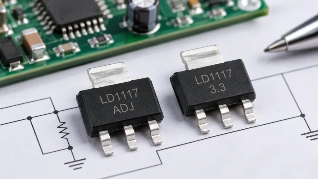
The main difference between LD1117-ADJ and LD1117-3.3 is how the output voltage is established. LD1117-ADJ uses an external resistor divider to set the output, while LD1117-3.3 provides a fixed 3.3V rail without programming resistors.
The adjustable version can also be configured for approximately 3.3V, so the choice is not simply about output voltage. It also affects circuit complexity, minimum-load requirements, PCB connections, and how easily the regulator can be substituted into an existing design. For a dedicated 3.3V rail, the fixed version is usually the simpler choice. For custom voltages or designs that need output flexibility, LD1117-ADJ is more suitable.
What Is the Difference Between LD1117-ADJ and LD1117-3.3?
Both versions belong to the same LD1117 regulator family and share many basic characteristics, including an output capability of up to 800mA and similar dropout behavior. The practical difference begins at the feedback connection: the adjustable version expects an external network to define the output, while the fixed version is internally configured for 3.3V.
That distinction affects more than the schematic. It changes what Pin 1 does, how many external components are required, what happens at very light loads, and how much flexibility the designer has if the required rail changes later.
Output Setting and Circuit Differences
For LD1117-ADJ, Pin 1 is the ADJ pin. A resistor divider between VOUT, ADJ, and ground determines the final voltage. The circuit therefore needs at least two programming resistors in addition to the input and output capacitors.
For LD1117-3.3, Pin 1 serves as GND. The internal voltage-setting network is already configured for 3.3V, so no external divider is needed. This reduces the number of design variables and makes the fixed version attractive when the rail will always remain at 3.3V.
The practical distinction can be summarized as follows:
| Feature | LD1117-ADJ | LD1117-3.3 |
|---|---|---|
| Output voltage | Adjustable | Fixed 3.3V |
| Voltage setting | External resistor divider | Internally set |
| Pin 1 function | ADJ | GND |
| Programming resistors | Required | Not required |
| Minimum-load specification | 2mA typ., 5mA max. | Characterized down to 0mA |
| Circuit complexity | Higher | Lower |
| Voltage flexibility | High | None |
| Typical use | Custom or flexible rail | Dedicated 3.3V rail |
Key Electrical Differences
The adjustable LD1117 uses a nominal 1.25V reference between the OUT and ADJ pins. The standard version is specified at 1.238V to 1.262V at 25°C under the stated test conditions. It also specifies a minimum load current of 2mA typical and 5mA maximum.
The fixed 3.3V version is specified at 3.267V to 3.333V at 25°C and 10mA load, while its broader operating specification covers 3.235V to 3.365V over the stated input and 0-to-800mA load conditions.
These figures should not be interpreted as one version simply being “better” than the other. The fixed device removes the external feedback network from the voltage-setting process, while the adjustable version gives the designer control over the final output. The right choice therefore depends on whether simplicity or voltage flexibility matters more in the circuit.
How Can LD1117-ADJ Be Set to 3.3V?
LD1117-ADJ does not require a special 3.3V version to produce a 3.3V rail. Instead, its output is established by selecting the resistor divider around the ADJ pin.
This makes the adjustable part useful when the design may need a non-standard voltage, when several product variants share the same PCB, or when the final rail value may change during development. The calculation itself is straightforward, although real component tolerances still need to be considered.
Output Voltage Formula
The output voltage is defined by:
VOUT = VREF × (1 + R2 / R1) + R2 × IADJ
For the LD1117 adjustable version, the typical values are:
- VREF = 1.25V
- IADJ = 60µA
- R1 is normally set to 120Ω
The datasheet notes that R2 is generally in the kilohm or lower range, so the R2 × IADJ term may be small enough to ignore for a first-pass calculation. However, it should not be treated as nonexistent when output accuracy matters. ST also recommends placing the feedback resistors carefully so the divider senses the output and load return properly rather than picking up avoidable PCB voltage drops.
For a quick estimate, the equation is often simplified to:
VOUT ≈ VREF × (1 + R2 / R1)
This simplified form is useful for selecting an initial resistor pair, while the complete equation should be used when checking the expected nominal output.
A Practical 3.3V Example
If R1 is kept at the commonly recommended 120Ω value, an R2 value close to 196Ω produces approximately 3.3V.
Using the complete equation with typical device values:
VOUT = 1.25 × (1 + 196 / 120) + 196 × 0.00006
VOUT ≈ 3.303V
So a practical example is:
- R1 = 120Ω
- R2 = 196Ω
- Calculated typical output ≈ 3.303V
This does not mean every assembled board will measure exactly 3.303V. The final voltage is affected by the regulator reference tolerance, adjustment-pin current, resistor tolerance, temperature, and normal line and load regulation.
The useful conclusion is simpler: LD1117-ADJ can be configured for a 3.3V rail without difficulty, but doing so introduces an external feedback network that the fixed 3.3V version does not require.
If LD1117-ADJ Can Output 3.3V, Why Choose LD1117-3.3?
If both parts can ultimately produce about 3.3V, the fixed version still has an important advantage in designs where 3.3V is a permanent requirement: it removes unnecessary design variables.
LD1117-3.3 does not require the external R1/R2 divider, so there are fewer components to place, fewer tolerance contributors to consider, and less feedback routing around the regulator. For a straightforward 5V-to-3.3V logic or MCU rail, that usually makes the schematic and PCB easier to review and reproduce.
The adjustable version becomes more useful when voltage flexibility is intentional. A prototype may need the rail changed during development, or the same PCB may be used for several product variants that require different output voltages. In those cases, keeping the adjustable regulator and changing resistor values can be more convenient than maintaining a separate fixed-voltage regulator for every variant.
The trade-off is therefore not “fixed is better” or “adjustable is better.” It is more useful to think of them this way: LD1117-3.3 minimizes design complexity, while LD1117-ADJ maximizes output flexibility. If the circuit will never need anything other than 3.3V, the extra flexibility of the adjustable version may provide little practical benefit.
Can LD1117-ADJ Directly Replace LD1117-3.3?
Not automatically. The common package versions use the same basic pin positions, but Pin 1 has a different electrical role. For SOT-223, DPAK, and TO-220 versions, Pin 2 is VOUT, Pin 3 is VIN, and the tab is also connected to VOUT. Pin 1 is ADJ on the adjustable version and GND on the fixed version.
That means a device may physically fit the same footprint while still being electrically incompatible with the existing circuit. If you need to verify package dimensions, pin assignments, or PCB footprint differences in more detail, this SOT package guide provides a broader reference for common SOT packages. A board designed for LD1117-3.3 normally connects Pin 1 directly to ground, whereas LD1117-ADJ requires a feedback divider. Installing the adjustable part without providing that network does not reproduce the fixed 3.3V circuit.
Before treating one version as a replacement for the other, check:
- Package and footprint
- Pin 1 connection
- Feedback resistor network
- Required output voltage
- Input and output capacitor arrangement
- Expected load and thermal conditions
For broader substitution work, an electronic parts cross reference can help identify candidate alternatives, but package similarity alone should never be treated as proof of electrical compatibility.
The practical rule is simple: the package may fit, but the circuit may not. Replacement should be evaluated at the schematic and application level, not only by comparing the LD1117 family name or package outline.
Minimum Load and Output Regulation
The adjustable and fixed versions also differ at very light load. For LD1117-ADJ, the datasheet specifies a 2mA typical and 5mA maximum minimum load current. By comparison, the fixed 3.3V version is characterized over a load range extending down to 0mA under its stated test conditions.
In practice, this difference matters mainly when the regulator may spend significant time with almost no load. A normal logic rail supplying a continuously active circuit may already draw enough current that the minimum-load requirement is not the dominant design concern. A standby rail, lightly loaded test circuit, or design in which downstream circuitry can shut down almost completely deserves more attention.
The important point is not that the adjustable version is unsuitable for light loads. It is that its specified regulation conditions include a minimum-load requirement that should be checked rather than assumed away. This is another reason to evaluate the exact regulator version instead of treating all LD1117 variants as electrically identical.
5V-to-3.3V Dropout and Thermal Limits
A common use case is regulating a 5V supply down to 3.3V. In this case, the available voltage headroom is:
VIN − VOUT = 5V − 3.3V = 1.7V
The LD1117 datasheet lists typical dropout voltage of about 1.0V at 100mA, 1.05V at 500mA, and 1.10V at 800mA. Under those conditions, a stable 5V input normally provides sufficient voltage headroom for a 3.3V output.
The more important constraint at higher current is often heat rather than dropout. For a linear regulator, a useful first estimate is:
P ≈ (VIN − VOUT) × IOUT
For a 5V-to-3.3V conversion:
| Load Current | Approx. Regulator Power Dissipation |
|---|---|
| 100mA | 0.17W |
| 300mA | 0.51W |
| 500mA | 0.85W |
| 800mA | 1.36W |
At 500mA, the regulator must already dissipate about 0.85W as heat. At 800mA, that rises to approximately 1.36W. This is why the stated 800mA output capability should not be interpreted as a guarantee that every SOT-223 board can continuously deliver 800mA under every input voltage and ambient condition.
Package choice, PCB copper area, ambient temperature, and airflow all affect junction temperature. The LD1117 datasheet, for example, lists different junction-to-ambient thermal resistance values for SOT-223, DPAK, SO-8, and TO-220 packages. A larger copper heat-spreading area can improve the thermal path of an SOT-223 package, but the required layout should be determined from the actual board and operating conditions rather than from a universal copper-area rule.
Output Capacitor Requirements
The current LD1117 datasheet specifies a minimum 10µF output capacitor for stability, and its typical fixed-output application circuit also shows a 10µF output capacitor. This is the appropriate starting point when designing around the LD1117 itself.
Capacitor type also deserves attention. Later technical guidance from ST recommends at least 22µF for adjustable variants and cautions that very-low-ESR ceramic capacitors should not simply be substituted without considering regulator stability. For a production design, the safest approach is to verify the capacitor network against the latest device-specific guidance and validate the regulator under expected load and temperature conditions.
This is particularly important when replacing another regulator from the broader 1117 family. Similar part numbers do not guarantee identical capacitor or ESR requirements, so capacitor recommendations from another 1117 device should not automatically be copied into an LD1117 design.
Which Should You Choose: LD1117-ADJ or LD1117-3.3?
For a design that permanently needs a 3.3V rail, LD1117-3.3 is usually the more direct choice. It removes the external voltage-setting divider, reduces the number of components involved in establishing VOUT, and avoids introducing resistor tolerances and feedback routing into a function that does not need to be adjustable.
LD1117-ADJ becomes more useful when voltage flexibility is part of the requirement rather than an accidental extra feature. This can include prototype boards, custom voltage rails, or one PCB platform that supports several output-voltage variants by changing resistor values.
| Design Situation | Better Fit | Main Reason |
|---|---|---|
| Fixed 3.3V MCU or logic rail | LD1117-3.3 | Simpler voltage-setting circuit |
| Custom output voltage | LD1117-ADJ | Adjustable output |
| Prototype with changing rail requirements | LD1117-ADJ | Easy voltage changes |
| One PCB for several voltage variants | LD1117-ADJ | Output can be changed through divider values |
| Existing fixed 3.3V PCB | LD1117-3.3 | Avoid feedback-network redesign |
| Component substitution | Check the circuit first | Package similarity alone is insufficient |
| Very lightly loaded rail | Check carefully | ADJ minimum-load requirement matters |
The decision can therefore be reduced to one practical rule: choose LD1117-3.3 when 3.3V is a permanent requirement and circuit simplicity matters; choose LD1117-ADJ when output-voltage flexibility is part of the design requirement.
For new designs with unusually strict battery-life, standby-current, efficiency, or thermal targets, the regulator itself should also be evaluated against those system requirements rather than selected only because the 1117 family is familiar. This does not make the LD1117 unsuitable by default; it simply means the regulator should match the actual application.
For projects that also involve component sourcing, BOM review, or replacement verification, China Chip Depot can support semiconductor selection and compatibility checks after the electrical requirements have been defined.
FAQs
Can LD1117-ADJ be set to 3.3V?
Yes. LD1117-ADJ uses an external resistor divider to set the output. With R1 = 120Ω and R2 = 196Ω, the calculated output using typical device values is approximately 3.303V.
Can LD1117-ADJ directly replace LD1117-3.3?
Not automatically. Pin 1 is ADJ on the adjustable version and GND on the fixed version, so the existing PCB and feedback network must be checked before substitution.
Is 5V input enough for LD1117-3.3?
Usually yes from a dropout-voltage perspective. A 5V input provides about 1.7V of headroom above 3.3V, but thermal dissipation becomes increasingly important as load current rises.
Does LD1117 need an output capacitor?
Yes. The current datasheet specifies at least 10µF at the output for stability. Adjustable designs should also consider the more conservative capacitor guidance discussed above.
Can LD1117 continuously supply 800mA?
Not under every operating condition. Continuous current capability depends on VIN − VOUT, package, PCB thermal design, ambient temperature, and the resulting junction temperature.
Conclusion
LD1117-ADJ and LD1117-3.3 solve slightly different design problems. The adjustable version provides voltage flexibility through an external feedback divider, while the fixed version provides a simpler path to a permanent 3.3V rail.
LD1117-ADJ can be configured for approximately 3.3V, but that does not make the two versions automatically interchangeable. Pin 1 usage, feedback components, minimum-load behavior, capacitor requirements, and thermal conditions still need to be checked. For a dedicated 3.3V supply, LD1117-3.3 is usually the simpler option; when output flexibility is genuinely required, LD1117-ADJ is the more appropriate choice.