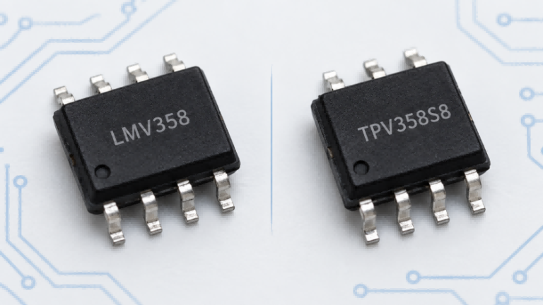
LMV358IDR and LMV358DR2G are both dual, low-voltage operational amplifiers with rail-to-rail outputs, and their headline specifications are close enough that they are often considered potential substitutes. They share the same basic function, an 8-pin SOIC format, a 2.7 V to 5.5 V supply range, and similar bandwidth and slew-rate performance.
However, similar specifications do not automatically make two op amps universally interchangeable. For an existing design, the key questions are whether the pinout and PCB footprint are compatible and whether differences in input bias current, offset limits, temperature rating, and actual operating conditions matter in the circuit. This comparison focuses on those replacement decisions rather than simply listing every available datasheet parameter.
LMV358IDR vs LMV358DR2G: Can They Be Direct Replacements?
In many general-purpose LMV358 circuits, LMV358IDR and LMV358DR2G can be considered potential pin-compatible alternatives, but the substitution should be treated as conditional rather than automatically approved. Their basic function, pin arrangement, supply-voltage range, gain bandwidth, slew rate, and rail-to-rail output behavior are closely aligned.
The most important differences are not the basic headline specifications. LMV358DR2G has a much lower typical input bias current, while LMV358IDR is specified across a wider operating-temperature range. Those differences may have little practical effect in a low-impedance buffer operating at room temperature, but they can become important in high-impedance sensor circuits or equipment expected to operate above 85°C.
| Compatibility Check | LMV358IDR vs LMV358DR2G | Replacement Impact |
|---|---|---|
| Basic function | Highly similar | Low risk |
| Pinout | Compatible | Strong compatibility |
| Package class | 8-pin narrow-body SOIC | Verify actual PCB land pattern |
| Supply range | 2.7 V to 5.5 V for both | Low risk |
| Gain bandwidth | 1 MHz for both | Low risk |
| Slew rate | 1 V/µs for both | Low risk |
| Input common-mode behavior | Very similar | Usually low risk |
| Output swing | Very similar | Load-dependent |
| Input bias current | Meaningfully different | Important with high source impedance |
| Operating temperature | Meaningfully different | Important in high-temperature designs |
| Overall replacement | Conditional | Verify actual circuit requirements |
The right question is therefore not simply whether the two part numbers “match.” The more useful question is whether their differences remain within the electrical, accuracy, and environmental limits of the specific circuit.
Key Specifications Comparison
Both devices belong to the broader category of low-voltage operational amplifiers used for buffering, signal conditioning, sensing, and other analog functions. A useful replacement comparison should focus on parameters that can actually change circuit behavior rather than procurement details such as reel quantity, plating description, or database publication date.
The table below concentrates on functional, electrical, mechanical, and environmental specifications. Values should always be interpreted together with their test conditions; a typical specification and a guaranteed maximum value are not interchangeable.
| Parameter | LMV358DR2G | LMV358IDR | Replacement Relevance |
|---|---|---|---|
| Amplifier channels | 2 | 2 | Same function |
| Supply voltage range | 2.7 V to 5.5 V | 2.7 V to 5.5 V | Closely aligned |
| Output type | Rail-to-rail | Rail-to-rail | Closely aligned |
| Input common-mode range at 5 V | About 0 to 4 V guaranteed | About 0 to 4 V guaranteed | Closely aligned |
| Input offset voltage | 1.7 mV typ; up to 9 mV under specified conditions | 1.7 mV typ; 7 mV max at 25°C, higher over full temperature | Application-dependent |
| Input bias current | <1 nA typ | About 15 nA typ at 25°C | Major difference |
| Supply current, dual device | About 210 µA typ | About 210 µA typ | Very similar |
| Gain bandwidth product | 1 MHz typ | 1 MHz typ | Same class |
| Slew rate | 1 V/µs typ | 1 V/µs typ | Same class |
| Output swing | Rail-to-rail behavior; load-dependent | Rail-to-rail behavior; load-dependent | Very similar |
| Operating temperature | -40°C to +85°C | -40°C to +125°C | Major difference |
| Package | 8-pin narrow-body SOIC | 8-pin SOIC, D package code | Closely aligned |
| Lead pitch | 1.27 mm | 1.27 mm | Strong compatibility |
| Pin count | 8 | 8 | Same |
Most of the specifications that first attract attention are therefore not major replacement barriers. Supply range, bandwidth, slew rate, supply current, and general input/output behavior are all closely aligned.
The two differences that deserve the most attention are input bias current and operating-temperature rating. Input offset voltage also deserves review in precision circuits, but it should be compared using the same temperature and test conditions rather than by placing unrelated maximum and typical figures side by side.
Are the Pinout and SOIC-8 Packages Compatible?
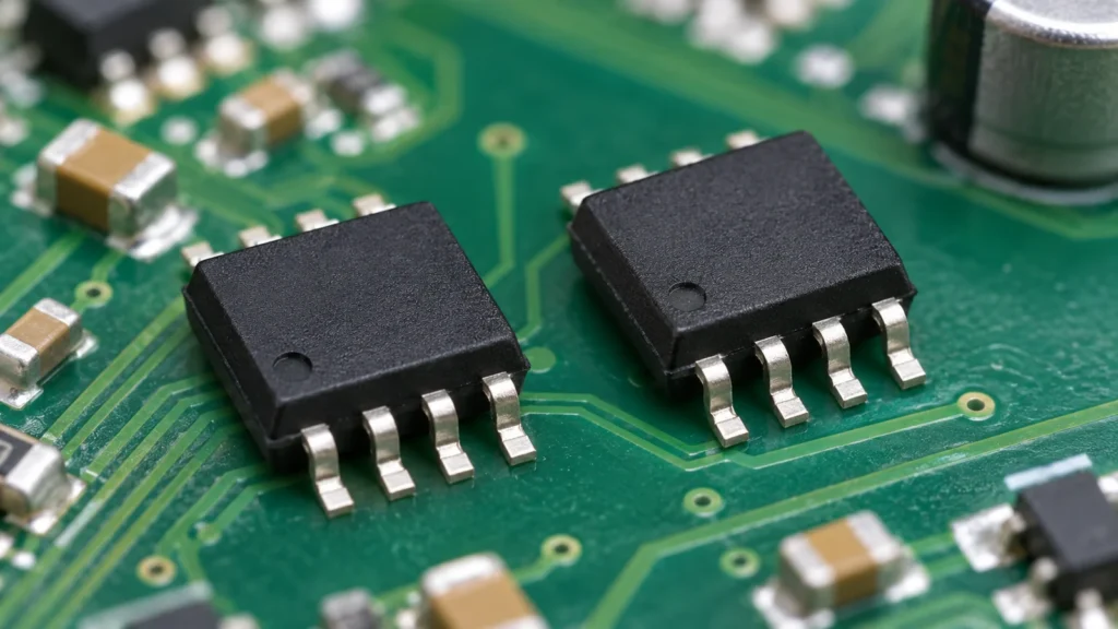
Package naming can make these two devices appear more different than they actually are. LMV358DR2G is commonly specified as an 8-pin SOIC device, while LMV358IDR uses an SOIC package identified by the package code “D.” That letter is a package drawing designation rather than evidence that the device belongs to a completely different footprint family.
Both devices use an 8-pin narrow-body SOIC format with a 1.27 mm lead pitch, and their package dimensions fall within the normal range for this package class. The functional pin arrangement is also the same:
| Pin | Function |
|---|---|
| 1 | OUT A |
| 2 | IN− A |
| 3 | IN+ A |
| 4 | V− |
| 5 | IN+ B |
| 6 | IN− B |
| 7 | OUT B |
| 8 | V+ |
This makes the two devices pin-compatible at the functional level. It also means that package names alone should not be used to conclude that a PCB redesign is required.
For an existing production board, however, package compatibility should still be confirmed against the actual package drawings and land pattern used in the PCB library. Small differences in maximum body or lead dimensions are normal between package specifications, and the board footprint—not the text label used in a component database—is the final physical reference.
Which Electrical Differences Actually Matter?
Once supply voltage, pinout, and package compatibility have been checked, the replacement decision becomes much more application-specific. Many specifications are nearly identical, so the useful engineering question is not how many numbers differ but which differences can actually change circuit behavior.
For these two devices, three areas deserve particular attention: input bias current, operating-temperature range, and the smaller differences in DC precision. Other commonly compared parameters such as 1 MHz gain bandwidth and 1 V/µs slew rate are closely aligned and are unlikely to be the main reason to reject a substitution in a typical low-frequency LMV358 application.
Input Bias Current Is the Largest Electrical Difference
The most obvious electrical difference is input bias current. LMV358DR2G is specified with a typical input bias current below 1 nA, while LMV358IDR is around 15 nA typical at room temperature. The difference reflects the way their input stages are implemented, but the internal transistor technology itself is less important to most users than the effect it has on the circuit.
Input bias current becomes more important as the resistance seen by the amplifier input increases. A useful first-order estimate is:
Input error ≈ input bias current × source resistance
For example, with a source resistance of 100 kΩ, 1 nA of bias current corresponds to roughly 0.1 mV of input error, while 15 nA corresponds to about 1.5 mV. This does not mean that every circuit will see exactly those errors, but it shows why a specification that appears small can become relevant when the source impedance is high.
In a low-resistance buffer or a circuit driven from a low-impedance source, the difference may have little practical effect. In a high-impedance sensor interface, resistor-divider measurement, or other weak-signal DC circuit, input bias current deserves much more attention before approving the substitution.
Temperature Range Can Limit Substitution
The operating-temperature rating creates a clearer boundary. LMV358DR2G is specified for operation from -40°C to +85°C, while LMV358IDR is specified from -40°C to +125°C in the current official device specifications.
For equipment operating in ordinary indoor conditions or environments that remain comfortably below 85°C, this difference may not affect the design. The situation changes when the original circuit has been qualified for elevated ambient temperatures, is installed near a significant heat source, or is expected to operate continuously in a hotter industrial enclosure.
If the design requirement extends beyond +85°C, LMV358DR2G should not be treated as an equivalent replacement for LMV358IDR based on rated operating temperature. The correct decision is determined by the required environmental specification, not by the fact that the two devices otherwise have similar electrical performance.
Offset, Common-Mode Range and Output Swing Are More Similar
Input offset voltage deserves review in precision DC circuits, but the comparison is more nuanced than a simple “7 mV versus 9 mV” statement. Both devices have a typical offset around 1.7 mV. The maximum values differ depending on temperature and test conditions, so the relevant comparison is whether the worst-case offset still fits the circuit’s error budget.
Their input common-mode behavior is also closely aligned. At a 5 V supply, both have a guaranteed input range that reaches from around ground to approximately 4 V rather than all the way to the positive supply rail. This is an important practical limitation because rail-to-rail output does not mean rail-to-rail input. A sensor signal that approaches VCC must therefore be checked against the input common-mode limit regardless of which of the two devices is used.
Output swing is similarly close between the two parts. Both are rail-to-rail-output amplifiers, but neither should be interpreted as producing exactly 0 V and VCC under every load. The remaining voltage from each rail depends on supply voltage and output load. In a light-load circuit, the output can move closer to the rails; under a heavier load, more headroom is required. For replacement purposes, the important point is that their specified output behavior is broadly similar rather than a major differentiator.
Can LMV358IDR Replace LMV358DR2G in Different Applications?
The practical replacement risk depends less on the shared LMV358 name and more on how the op amp is being used. A circuit with a low-impedance source, moderate temperature, and signals comfortably inside the supply rails places very different demands on the device than a high-impedance sensor interface or equipment operating near its temperature limit.
The table below summarizes where the differences discussed above are most likely to matter.
| Application | Replacement Risk | Main Parameter to Check |
|---|---|---|
| General-purpose buffer | Low | Normal input and output operating range |
| High-impedance sensor interface | Moderate | Input bias current |
| ADC or battery monitoring | Moderate | Offset, common-mode range, output swing |
| High-temperature industrial equipment | High if operation exceeds 85°C | Operating-temperature rating |
General-Purpose Buffer
For a general-purpose voltage buffer or low-frequency amplification stage driven from a relatively low source resistance, LMV358IDR and LMV358DR2G are often close substitutes. Their supply range, bandwidth, slew rate, pinout, and general input/output behavior are closely matched.
If the signal remains comfortably inside the valid common-mode range and the equipment operates within the temperature rating of both parts, the lower input bias current of LMV358DR2G may have little practical impact. This is the type of circuit in which the two devices are most likely to behave similarly without requiring substantial redesign.
High-Impedance Sensor Interface
A high-impedance sensor interface deserves more attention because the source resistance can magnify the effect of input bias current. In this situation, the much lower typical bias current of LMV358DR2G can reduce one source of DC measurement error.
That does not automatically make it the better device for every sensor circuit. Offset voltage, signal range, temperature, and the total error budget still matter. The key point is that source impedance changes the importance of the bias-current difference, so a substitution that is uneventful in a low-impedance buffer may require closer review in a resistive sensor network.
ADC or Battery Monitoring
In an ADC front end or battery-monitoring circuit, the first checks should be whether the input voltage remains inside the common-mode range and whether the amplifier can drive the required output voltage under the expected load. Both devices have very similar limits in these areas, so neither has an obvious universal advantage.
Offset voltage becomes more important when the measured signal is small or when the circuit requires tight DC accuracy. In that case, the correct approach is to evaluate the worst-case offset against the allowed measurement error rather than choosing a part solely from its typical specification.
High-Temperature Industrial Equipment
Temperature can become the deciding factor in equipment installed inside hot enclosures, near heat-generating components, or in other elevated-temperature environments. LMV358IDR is rated up to +125°C, while LMV358DR2G is rated up to +85°C.
For an application whose required operating range remains below +85°C, that difference may not affect the substitution. If the equipment has been designed or qualified for operation above that point, however, LMV358DR2G should not be treated as a temperature-equivalent replacement for LMV358IDR.
LMV358 Replacement Checklist
Even when two operational amplifiers appear highly compatible, a production substitution should be reviewed against the actual circuit rather than approved from a part-number comparison alone. The following checks cover the parameters most likely to affect an LMV358 replacement without turning the process into a full redesign review.
- Confirm the pinout. Make sure the two amplifier channels, supply pins, and inputs are assigned identically.
- Compare the package drawing and PCB land pattern. Do not reject or approve a replacement solely because one package is called SOIC-8 and another SOIC (D)-8.
- Confirm the supply-voltage range. Both devices support 2.7 V to 5.5 V, but the actual circuit supply should still be checked.
- Check the input common-mode voltage. Pay particular attention to signals approaching the positive supply rail.
- Check output swing under the expected load. Rail-to-rail output does not guarantee an ideal 0 V-to-VCC swing under every condition.
- Estimate bias-current error when source resistance is high.
- Check the offset-voltage allowance in precision DC measurements.
- Verify the required operating-temperature range.
For broader BOM substitution work, an electronic parts cross reference can help identify possible alternatives before package, electrical limits, and application conditions are reviewed. Final approval should still include prototype or board-level testing when the replacement will be used in production.
Which Part Should You Choose?
Neither device is universally better. The appropriate choice depends on which specification is more important in the actual circuit. LMV358IDR is the more suitable choice when the design requires operation above +85°C, or when an existing design has already been qualified around its wider specified temperature range.
LMV358DR2G can be attractive in standard-temperature applications where its very low typical input bias current is useful, particularly when the signal source has relatively high impedance. In ordinary low-voltage, low-frequency circuits with modest source resistance, the two devices may perform similarly enough that sourcing and existing BOM approval become more important than their small electrical differences.
For production sourcing, the safest approach is to choose the device that meets the original circuit requirements across voltage, temperature, accuracy, and load conditions rather than the one with the closest headline specifications.
Conclusion
LMV358IDR and LMV358DR2G are much closer substitutes than their different package naming may suggest. They share the same basic function, pinout, supply range, bandwidth class, slew rate, and broadly similar input and output voltage behavior.
The replacement becomes application-dependent mainly because LMV358DR2G has substantially lower typical input bias current, while LMV358IDR supports a wider specified operating-temperature range. For most designs, the best decision comes from checking those differences against the actual source impedance, signal range, accuracy requirement, load, and temperature environment rather than treating either device as universally interchangeable.
FAQs
Can LMV358IDR directly replace LMV358DR2G?
In many low-voltage general-purpose circuits, they can be considered potential pin-compatible substitutes. The replacement is still conditional because input bias current and operating-temperature ratings differ.
Are LMV358IDR and LMV358DR2G pin-compatible?
Yes. Both use the same functional 8-pin dual-op-amp pin arrangement.
Are SOIC-8 and SOIC (D)-8 the same package?
Not necessarily by name, but in this comparison both belong to the same narrow-body 8-pin SOIC package class. Actual package drawings and PCB land patterns should be compared rather than relying on the package label alone.
What is the main difference between LMV358IDR and LMV358DR2G?
The most important differences are input bias current and operating-temperature range. LMV358DR2G has much lower typical input bias current, while LMV358IDR is rated to a higher maximum operating temperature.
What is the LMV358 IC?
LMV358 is a dual, low-voltage operational amplifier family designed for 2.7 V to 5.5 V operation with rail-to-rail output. It is commonly used in low-voltage signal conditioning, buffering, sensing, and monitoring circuits.